Measure a Bipolar Signal with an Arduino Board

Arduino is a popular family of open source microcontroller boards. Hobbyists, students and engineers all over the world use this platform to quickly design and prototype a microcontroller driven circuit. One of its interfaces with the analog world is the ADC. Since these boards are mostly designed around an ATMEL ATmega32 or ATmega168 microcontroller, the ADC has 8 inputs and 10-bit resolution, making it suitable for many applications.

From time to time I receive a message through my Contact page with the question, how to interface a sensor, or an outside circuit with the Arduino ADC? In most cases the answer is an interface between a bipolar circuit and the Arduino board. As the bipolar circuit output varies from some negative to a positive level, the Arduino ADC cannot measure this signal directly, because the ADC inputs can only be between 0V and the reference voltage.

In one of these messages a reader asked me how to build an interface between a board that has an output voltage of -2.5V to +2.5V and the Arduino ADC. He told me that the Arduino reference voltage is AVCC = 5V. He would like to measure the +/-2.5V signal with the Arduino board and direct the microcontroller to take some action based on the result.

Read more

Using the Summing Amplifier as an Average Amplifier

Sometimes people ask how can one use a summing amplifier as an average amplifier. The answer is simple, provided that one knows what kind of average one needs.

The summing amplifier can output the average of two, three or more signals. This is different than a signal average. The summing amplifier cannot, for example, output the average of a triangle signal. For that, you need an integrator to perform the average in the analog realm, or you need to sample the signal and calculate the average with a microcontroller. This type of average is the signal average in the time domain. I will write an article about the average of a signal in a near future.

In this post I will show you how to average two or more signals with a summing amplifier. In How to Derive the Summing Amplifier Transfer Function I wrote that the summing amplifier shown in Figure 1

Read more

The Transfer Function of the Non-Inverting Summing Amplifier with “N” Input Signals

In a previous article, How to Derive the Summing Amplifier Transfer Function, I deduced the formula for the non-inverting summing amplifier with two signals in its input.  But what if we have 3, 4 or an n number of signals?  Can we add them all with one amplifier?

Theoretically, yes.  Practically, it is a different story.  There is a practical limit on how many signals can be summed up with one amplifier.  When the number of input signals grows, each signal component in the sum decreases in value. By the end of this article you will understand why.

summing_amplifier_1

Figure 1

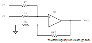
We already saw that, for a summing amplifier with two input signals (Figure 1), the transfer function is

image002 (1)

If we need to add 3 signals, the circuit schematic looks like the one in Figure 2.  What is the transfer function of this summing amplifier with 3 inputs?

Read more

How to Derive the Summing Amplifier Transfer Function

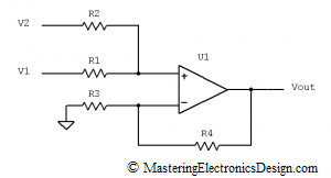
The summing amplifier, or the non-inverting summing amplifier, is an analog processing circuit with the transfer function (the summing amplifier formula as some say) shown in the following equation.

image001 (1)

The first term of the product is the actual summing, while the second term is a gain due to the R3 and R4 resistors.  I prefer this type of summing amplifier as shown in Figure 1, because it is more flexible and allows us to achieve any linear function we want.

summing_amplifier1

Figure 1

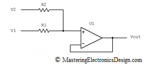
Some authors prefer the following schematic,

summing_amplifier2

Figure 2

with the transfer function

image0041 (2)

One can see that the summing amplifier in Figure 2 is a subset of my preferred schematic in Figure 1.  In Figure 2, R4 is zero, while R3 is infinity (open connection).  It performs the analog summation between V1 and V2, with a gain of 1.  Therefore, the amplifier in Figure 1 gives us more choices when designing a function with this circuit.  If the gain is not needed, this should come up from calculations, as in this article Solving the Summing Amplifier.

If you followed this website, by now you probably figured that I am not a promoter of learning formulas by heart.  I like to derive the transfer function if I need it. So, how do we prove this formula?

We will use the Superposition Theorem, which says that, the effect of all the sources in a circuit is equal with the sum of the effects of each source taken separately in the same circuit.  Therefore, if we take out one source, V2, and replace it with a wire, we then can find the voltage in each node and the current in each branch of this circuit due to the remaining source V1.  Then we do the same with V1 and then sum up the currents on each branch and the voltage levels on each node.  We are only interested in Vout, so this should be simple.

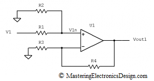
We will first make V2 = 0V, by connecting R2 to ground, as in Figure 3.

summing_amplifier3

Figure 3

The Op Amp is considered an ideal component, so that the input bias currents are negligible.  If the current in the non-inverting input is zero, R1 and R2 make a voltage divider for V1.  The non-inverting input voltage V1n, can be written as

image0061 (3)

and, based on the non-inverting amplifier transfer function, Vout1 is

image0071 (4)

By replacing V1n in (4), the output voltage is

image0082 (5)

In the second part of my demonstration, based on the Superposition Theorem, R2 is connected back to V2 and V1 = 0, by connecting R1 to ground.  Following the same train of thought Vout2 can be written as

image0091 (6)

Now we have to add Vout1 to Vout2 to complete the third step of the Superposition Theorem.  After factorizing the gain component 1+R4/R3, the summing amplifier transfer function becomes the mathematical relation shown in (7).

image001 (7)

Q.E.D.

>>>  <<<

This formula shows that this sum is a weighted sum between V1 and V2.  This is better than a direct sum V1 plus V2, because, again, brings flexibility in design.  Together with the differential amplifier, this circuit brings another treat in the art of electronics design.

Solving the Summing Amplifier

How to Design a Summing Amplifier Based on the Input and Output Voltage Level Requirements

In allaboutcircuits.com forum a member asked how can he drive a MOSFET that needs a voltage range of 4V to 5V with a DAC with the output range of 0V to 5V?

Initially I thought he should use a differential amplifier.  However, based on the articles I published, MasteringElectronicsDesign.com: Solving the Differential Amplifier – Part 1, Part 2 and Part3 the solution based on a differential amplifier would require a negative voltage level in the input.   Although V1 can be the input from 0V to 5V, V2 has to be negative, so that the output shifts to positive values.

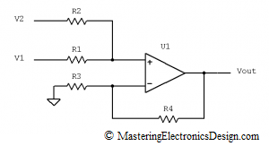
Then I thought of the Summing Amplifier, or the Non-Inverting Summing Amplifier, which is shown in Figure 1.  It is called a summing amplifier, because two signals are summed in one of the amplifier inputs.  In this case, V1 and V2 are summed in the non-inverting input.
summing_amplifier1Figure 1

The summing of V1 and V2 is not direct.  Resistors R1 and R2 make a weighted sum and this is what makes this amplifier very useful.  As in the case with the differential amplifier, one can use this circuit to achieve any linear function.  This article shows you how to design a summing amplifier based on the input and output requirements.  You can also solve your amplifier with the calculator I posted here:  MasteringElectronicsDesign.com: Summing Amplifier Calculator.

The transfer function of the summing amplifier is as follows.

image002 (1)

You can find its demonstration in this article, MasteringElectronicsDesign.com: How to Derive the Summing Amplifier Transfer Function.

Let’s write down what we know:

If Vin1 = 0V then Vout1 = 4V and
If Vin2 = 5V then Vout2 = 5V,

where by Vin1 and Vin2 I noted the input range limits, and by Vout1 and Vout2 I noted the output range limits.

Let’s choose one of the summing amplifier inputs to be Vin, say V1.

Because we have two instances that we know, Vin1 and Vin2 and the corresponding outputs, Vout1 and Vout2, let’s rewrite equation (1) using these two instances.

image0072 (2)

This is a linear system of two equations with a lot of unknowns: R1, R2, R3, R4 and V2.  However, we can simplify our life by grouping the resistors in ratios.  The equations can be rewritten like this,

image0081 (3)

where by k1 and k2 I noted:

image0091 (4)

Now we are left with three unknowns, k1, k2, V2.  I can simply consider V2 as a known value, because I can connect to R2 any voltage I want or, more conveniently, a voltage that I already have in the circuit.  I will target for V2 = 5V, since there is already a DAC in this circuit with an output range of 0 to 5V.  So I can assume there is a 5V reference in this circuit.

If k1 and k2 are the remaining unknowns, then (3) is a system of two equations and two unknowns as in (5), which can be easily solved.

image0103 (5)

It can be easily seen that the second equation becomes

image0111 (6)

so k2 has to be zero.

The result is k1 = 1/4 and k2 = 0.

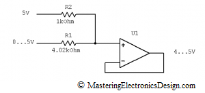
This result shows that we do not need the resistors R3 and R4. Also, the ratio between R2 and R1 is 1/4.  We can choose R2 = 1 kohm and a standard value for R1 = 4.02 kohm with a 1% tolerance.

The final circuit is shown in Figure 2.
circuitFigure 2

Since k2 is zero, R3 is zero, configuring U1 as a repeater for the summed voltage in the non inverting input.

Show Buttons
Hide Buttons
'