Articles on Internet and books show how to calculate the Least Significant Bit (LSB), but they take into consideration either the voltage reference (Vref) or the full scale (FS) of the ADC or DAC. Many times this leads to confusion, as a few messages I received from my readers show. Therefore, this article shows both ways of defining the LSB, so that people will have a clear understanding how to treat an ADC’s (Analog-to-Digital-Converter) or DAC’s (Digital-to-Analog-Converter) LSB.
What is an LSB? The LSB is the smallest level that an ADC can convert, or is the smallest increment a DAC outputs. Both converters are used at the boundaries between the analog and digital realms, making it possible for the analog circuits to talk to the digital ones and backwards.
To define an LSB, let’s not look, for the moment, at articles or text books. One of the recommendations I make is this: “When in doubt, read the manufacturer’s data sheet.” So, let us look at an ADC data sheet. The manufacturer writes in the data sheet all the information one needs about that particular component. Sure, nothing is perfect in this world, some info we need might not be there, but in the case of the LSB, I still have yet to see an ADC or DAC data sheet without the LSB definition in some form or another.
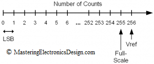
The ADC needs a voltage reference to convert an analog signal into a digital word. Depending on the number of bits it has, the ADC divides the voltage reference in small levels called counts. For example, if this is an 8-bit ADC, the counts will look like those in Figure 1. In an 8-bit ADC there are 28 = 256 counts.
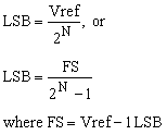
One count is 1 LSB, and is defined as follows:
| (1) |
where N is the ADC’s or DAC’s number of bits.
For ADCs that have a differential voltage reference, the LSB is
| (2) |
where Vref(+) and Vref(-) are the non-inverting and the inverting inputs of the differential voltage reference respectively.
The ADC outputs a digital word that shows how many counts are in its input voltage level. As the ADC counts the input level, it never reaches the voltage reference. Its full scale (FS) is calculated with the following formula:
| (3) |
After replacing the LSB in equation (3), the ADC full-scale results as in equation (4).
| (4) |
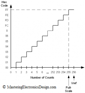
Figure 2 shows the ADC counts and the corresponding hex code.
In our 8-bit ADC example, if the voltage reference is Vref = 5V, then the LSB and FS are:
 |
(5) |
As you can see, and ADC can never reach its Vref but, as the number of bits is higher, it gets very close to its reference voltage. The same can be said about a DAC.
Moreover, from equation (1), we can write the mathematical relation between Vref and LSB as follows:
| (6) |
If we replace Vref in equation (3), and after calculations, we can write the definition of the LSB as a function of the ADC’s full-scale, as in equation (7).
| (7) |
This is the trouble, as the LSB has two definitions, equations (1) and (7). Both of them are valid, and some authors are ambiguous or confused about them. I have seen articles in which Vref is considered the component full-scale, which is the premise that generates subsequent wrong definitions.
Therefore, all one needs to remember about the LSB is its definition, as follows:
 |
(8) |
>>> <<<
Here are some data sheet examples:
AD7823, 8-Bit ADC, manufacturer Analog Devices
If Vref = 2.5 V then
1LSB = 9.766 mV,
FS = Vref – 1 LSB = 2.490234 V
If Vin = FS = 2.490234 V, then ADC Hex Code = FF, and
If Vin = 0 V, then ADC Hex Code = 00.
If Vref = 5 V then
1LSB = 19.531 mV,
FS = Vref – 1 LSB = 4.980469 V
If Vin = FS = 4.980469 V, then ADC Hex Code = FF, and
If Vin = 0 V, then ADC Hex Code = 00.
AD7685, 16-Bit ADC, manufacturer Analog Devices
If Vref = 2.5 V then
1LSB = 38.1 uV,
FS = Vref – 1 LSB = 2.499962 V
If Vin = FS = 2.499962 V, then ADC Hex Code = FFFF, and
If Vin = 0 V, then ADC Hex Code = 0000.
If Vref = 5 V then
1LSB = 76.3 uV,
FS = Vref – 1 LSB = 4.999924 V
If Vin = FS = 4.999924 V, then ADC Hex Code = FFFF, and
If Vin = 0 V, then ADC Hex Code = 0000.
DAC8830, 16-Bit DAC, manufacturer Texas Instruments
If Vref = 2.5 V then
1LSB = 38.1 uV,
FS = Vref – 1 LSB = 2.499962 V
If DAC Hex Code = FFFF, then Vout = FS = 2.499962 V, and
If DAC Hex Code = 0000, then Vout = 0 V.
If Vref = 5 V then
1LSB = 76.3 uV,
FS = Vref – 1 LSB = 4.999924 V
If DAC Hex Code = FFFF, then Vout = FS = 4.999924 V, and
If DAC Hex Code = 0000, then Vout = 0 V.


Thank you for this post. I needed to convert lsb to fs and searched on google. Boom, the second article on the first page. Thank you for doing this. Great website also.
Thank you for this article. It has cleared all my doubts regarding LSB.
Naveen and Chris. Thank you for your comments. I am glad you liked this article and the website in general.
I have been looking for clear explanation of this for some time. thank you very much for creating this article. 🙂
Super helpful!!! thanks a lot!!!
This was incredibly helpful and useful! Thanks 🙂
what if input signal range is given in stead of reference voltage and full scale voltage
ex: 0-10 v
Use equation 7 in this article to determine the least significant bit. At minimum, you need to know the number of bits the ADC is made for. If full scale is FS = 10V and the number of bits is, say, N = 12, LSB = FS / (2^N -1) which is 2.442 mV.
The input signal range will not help you because you need to know the ADC resolution to determine the LSB.
10 bit dac has a full scale output of 5v. if lsb changes by one bit what will be the change in output voltge
The output change is 1 LSB = 4.883 mV, and here is why:
Usually, the full scale is not 5V. The voltage reference, Vref, is. Manufacturers make the voltage reference a round number like 5V or 2.5V. So, if your 10-bit DAC has a voltage reference Vref = 5V, then the least significant bit is given by equation 1 in this article: LSB = Vref / 2^N = 5V / 2^10 = 4.883 mV.
Then the fulls scale, FS is given by equation 3: FS = Vref – 1 LSB = 5V – 4.883 mV = 4.99512 V.
Then the change in the output voltage by 1 LSB is deltaV = 4.883 mV.
Hi,
The quantization error from Fig 2 is 0-LSB. To make it +/-LSB/2 the curve can be shifted to left by LSB/2 (the so called mid-riser transfer curve). This reduces the FS range further by LSB/2 (VREF-1.5LSB).
My question is: can I redefine LSB as (VREF/2^N -1) so that my LSB increases a little but now I have FS range 0 to VREF?
Thanks.
Just to make it more clear the first and last bins would be LSB/2 and all bins in between will be LSB (VREF/2^N – 1).
In the case of the ADC, no. It measures the input voltage up to FF (for an 8-bit ADC), which will always be below Vref with an LSB.
In the case of the DAC, you can add an LSB at the DAC output to reach Vref. The range will be 1LSB to Vref. This is in theory. In practice, adding a few mV at the DAC output is impractical, because you will need an OpAmp and you will also add its offset.
Is one where to just use 6 of the most significant bits of a 12-bit ADC. What factors would change in the formula, for example what happens to the LSB?
If you use just the 6 most significant bits of a 12-bit DAC you will lower the resolution. Although you have a 12-bit DAC, it will behave like a 6-bit DAC. The LSB is recalculated with 6 bits, not 12-bits.
Let us look in the ADC 7641 data sheet. LSB = 2 x Vref/2^n.
How do you account for the fact that there is factor 2.
Thank you in advance,
Auren
AD7641 is a bipolar ADC. Take a look at page 16 of its datasheet. The reference voltage is 2.048V, and the ADC can convert input levels from -2.048V to +2.0479844V (which is FSR – 1 LSB). As such, the input span is 2*Vref and that is why, when calculating the LSB, one has to take into consideration Vref doubled.
this is awesome….
Well done, helped greatly thank you.
Well written. Helped a lot. Thank you.
How we can find Analog voltage corresponding to LSB for each of the ranges of
1}DAC 80
2}ADC 80
Thanks for your sharing, that helps a lot.
Still I have some confusions, wishing for your kind guidance.
First, even in the datasheet of AD7685, FSR is misused as REF on page 14. Is that so or I’m just mistaken?
Second, I get confused by the -0.5LSB shift in the transfer curve now. To my best knowledge, ADCs always perform the transfer curve as you mentioned before. I haven’t seen(or realized) where and how the -0.5LSB shift happened but it’s obviously everywhere in papers/articles. For instance, binary searching ADCs always start with comparing the input with Vref/2, which is the mid point of that step. If the input voltage is just slightly larger than Vref/2, the result would be 1, vice versa. But in the mid-riser transfer curve, the result should be the same. How to understand this?
Thanks again and hoping furthur answers.
Does it mean that for an ADC, the maximum input voltage that can be converted into digital code is FS ?
If the FS of ADC is 4.98V and I have to digitize a sinusoidal signal of 10V amplitude (peak). Then I have to attenuate my input signal by 4.98/10 to bring it within the FS of ADC. Correct ?
Yes, that is correct.
Great clarification, solved my question perfectly.
Great and clear explanation. Thank you so much.
such a helpful contents.
thanks a lot for your efforts to bring these information to us.
best wishes.
I read that resolution is weight of an lsb, is it correct?
coz for resolution we use Vr/step size
“I read that resolution is weight of an lsb, is it correct?”
Resolution is 2^N so it is 1 divided by the weight of an LSB.
“for resolution we use Vr/step size”
Correct, assuming that Vr is the reference voltage and step size has units volts (or micro volts). The same as equation (1) in this article.
Thank you for the article
So, the only correct equation to calculate voltage from any ADC reading is:
Vin = (Vref/2^N) x ADC + (Vref/2^N)
It is actually
Vin = (Vref/2^N) x ADC – (Vref/2^N)
Here is an example: If Vin is at Full Scale (FS), then
Vin = FS = (Vref/2^N) x 2^N – (Vref/2^N) = Vref – 1LSB (as in equation 8 in this article)
The lower ADC reading, the bigger error (up to 50%) if you are using the following very common on the Internet equation:
Vin = (Vref/2^N-1) x ADC
Ok, I corrected the formula for 0V input voltage:
Vin = LSB x ADC + LSB x (ADC/ADC)
It is the same formula:
Vin = (Vref/2^N) x ADC – (Vref/2^N)
Here is for 0 volts input:
If Vin = 0, then the ADC code is 0, which is decimal 1 (2^0)
Then Vin = (Vref/2^N) x 2^0 – (Vref/2^N) = (Vref/2^N) x 1 – (Vref/2^N) = 0
El FSR =2.55V y el error es 0.1% FSR ¿Cuál es el error total del ADC de 8 bits? ¿Cuál es el LSB? ¿Cuál es el V máximo? ¿la resolución?
Gracias muy didáctico el artículo. Realmente fue de mucha ayuda.
Thank you for the great help!
I’m wondering whether now ADI changes the FS definition or not. Since from Table8 in AD7685 datasheet (https://www.analog.com/media/en/technical-documentation/data-sheets/AD7685.pdf), the code ‘FFFF’ corresponds to ‘FSR – 1LSB’ It seems that FSR (or FS !?) is the Vref in this article. Your response is much appreciated!
All rigth! one efect of knowedge and the tell very well comprensive. Many thank´s for article.