Power Supply Output Current Measurement with a Differential Amplifier
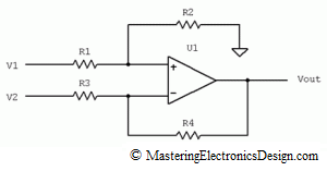
When designing a differential amplifier, part of the art is to manage the errors affecting the precision of the circuit. In MasteringElectronicsDesign.com: The Differential Amplifier Common-Mode Error – Part 1 of this presentation I discussed the common-mode error of a differential amplifier. I also showed that, given the circuit in Figure 1, the common-mode voltage can be viewed as V2, when we consider V1-V2 as a signal that rides on top of V2. The same goes for V1, which can be considered the common-mode voltage of the differential amplifier when -(V1-V2) is the signal that rides on top of V1.
Figure 1
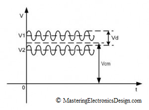
Most of the times, however, the input signals V1 and V2 would vary in time, whether there is an AC signal riding on top of a DC signal, or the input signals have a noise component as in Figure 2.
Figure 2
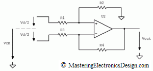
Because of that, it is customary to consider the common-mode voltage the average of the input signals, V1 and V2, as in Figure 3, so that the common-mode input signal lands in between V1 and V2.
Let’s note this signal with Vcm, and the difference V1-V2 with Vd.
| (1) |
From a signal difference point of view, each input will be referred to the common-mode voltage as shown in Figure 3. In this case, the difference signal Vd = (V1-V2) is split in two, so that the input R1 has a signal Vd/2 and the input R3 has a signal -Vd/2 as referred to the common-mode voltage Vcm.
What is the common-mode error in this case?
With these notations, I can express the input signals as in (2).
| (2) |
In MasteringElectronicsDesign.com: The Differential Amplifier Common-Mode Error – Part 1 I demonstrated that the output signal of the differential amplifier can be expressed as a function of V1-V2 and V2 as shown in (3).
 |
(3) |
By replacing V1 and V2 with the expressions (2), Vout becomes,
 |
(4) |
After calculations, the differential amplifier output becomes,
 |
(5) |
In equation (5), the first parenthesis is the differential gain and I will note it with Gd. The second parenthesis is the common-mode gain, noted with Gcm.
 |
(6) |
One can see that, if the resistor ratios are equal, Gcm is zero. We should note that this gain is the same as in the MasteringElectronicsDesign.com: The Differential Amplifier Common-Mode Error – Part 1, when the same expression multiplied V2. Indeed, this proves that, no matter the level of the common-mode voltage at the amplifier input, V2, Vcm or anything in between for that matter, the common-mode gain is the same.
Equation (5) also shows that the larger Vcm, the larger the common-mode error at the differential amplifier output. Since many times we cannot do anything about the common-mode voltage level, the electronics designer can only minimize the common-mode gain to reduce the error. This can be done by matching the resistor ratios.
One good example of using the differential amplifier is current measurement. One way is to measure the voltage drop across a small resistor. Another way is to measure the current inductively, with a magnetic probe.
Measuring the current through a network branch with a small resistor, called sense resistor, is preferred by many designers, because it can be very precise. Depending on the expected current level, the resistor value is chosen so that the voltage drop on this resistor is around a few hundred millivolts. A differential amplifier connected across the sense resistor amplifies the voltage drop to a manageable level, usually around 2.5V or 5V, so that an Analog to Digital Converter (ADC) can measure it with good resolution.
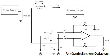
If the measurement has to be done at a power supply output (see Figure 4), the common mode voltage can be high, because it equals the power supply voltage level.
Figure 4
Let’s say that this is a 12V power supply that sources a nominal current of 5A to a system it powers. Based on the powered system functionality, the load current can vary in time and we need to monitor it. The voltage drop on Rsense has to be small enough so that the powered system still receives approximately 12V. If, instead of 12V, the system is powered at 11.9V, it can be good enough for most applications. Therefore, we can choose the drop on Rsense as 100mV. At 5A, the sense resistor has to be Rsense = 20 milliohms.
Also, let’s say we need to read the current with a microcontroller. For this, we need to use an ADC, with a reference voltage of 2.5V. We can design the differential amplifier resistors so that the nominal current of 5A means 2V at the amplifier output. This means that the nominal value is placed at 4/5th of the ADC range, so that there is some room for positive or negative load current variation.
If the resistor ratios are equal, the differential gain, Gd is
| (7) |
The gain of the differential amplifier has to be
| (8) |
Let’s choose R2 = R4 = 20 kohms and R1 = R3 = 1 kohm. What tolerances should I select for these resistors? Resistors with 1% tolerance are quite common nowadays and they are not expensive. With 1% tolerance resistors, what is the common-mode error?
Since V2 = Vpower, let’s choose equation (3) to calculate the output voltage, for a nominal power supply current of 5A.
 |
(9) |
With the tolerance t = 0%, the output is the ideal nominal value Vout = 2V.
When the tolerance is t = 1%, and in the worst case in which the resistor values may be as follows,
 |
(10) |
the output voltage is Vout = 2.413V. The extra 0.413V is the common-mode error which is significant, as it represents 20.6% of the nominal value.
What if we use resistors with 0.1% tolerance? For the worst case scenario described above, the output becomes Vout = 2.042V. The error of 42mV means that the power source current is measured with an error of 2.1%. Depending on the application requirements, this measurement may be good enough, or may not be acceptable. If the error is too high, the designer has to choose either better matched resistors, or choose instrumentation amplifiers. Analog Devices’ AD620 can do the job with high precision.
There are some other questions that rise from this experiment:
Can the common-mode voltage damage the operational amplifier used for the differential amplifier circuit?
Is the sense resistor small enough so that the differential amplifier components do not modify its value and generate errors?
Is the offset voltage of the differential amplifier small enough so that the output offset does not appear as an error?
Are the operational amplifier input bias currents small enough, or their offset for that matter, so that there are no perceived errors at the amplifier output?
Is the temperature coefficient of the differential amplifier components small enough so that any temperature variation does not result in measurement errors?
I will discuss all these possible errors in future articles. Stay tuned.


