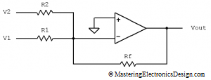
The inverting summing amplifier does exactly what its name says: adds the input signals and inverts the result. This amplifier presents a major advantage versus the non-inverting summing amplifier. The input signals are added with their own gain. The disadvantage is the inversion of the sum, which might not be desirable in some cases.
Figure 1
Figure 1 shows the non-inverting summing amplifier with two inputs. Its transfer function is shown in equation (1).
| (1) |
As you can see, this is a simple function. Each signal is added with its own gain created by the feedback resistor, Rf, and the corresponding resistor for that signal. But, why is that? Why is this transfer function a lot simpler than the non-inverting summing amplifier? How can we derive this function? What is the transfer function of the inverting summing amplifier with 3, 4, or n inputs? This article answers all these questions.
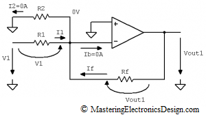
Using the Superposition Theorem, let’s start by making V2 zero as in Figure 2.
Figure 2
The key point here is to understand that the voltage level at the inverting input of the operational amplifier is zero volts. If this is clear to you, the rest is really simple. In the electronics jargon, it is said that the node is a virtual ground. It is called like that because it presents zero volts, without being galvanically connected to ground.
But why is the inverting input zero volts?
Because the non-inverting input is connected to ground. The Op Amp will set the output level at a voltage that will bring its inverting input at the same level as the non-inverting input. This is due to the Op Amp’s very high differential gain, on the order of 100,000. If the output is at a few volts, say 5 V, the differential voltage at the Op Amp input has to be
| (2) |
With a few tens of microvolts between the operational amplifier inputs, the inverting and non-inverting inputs can be considered at the same potential, hence the virtual ground.
The virtual ground in the inverting input helps determine the voltage drop on the feedback resistor Rf. Since the inverting input is at zero volts, the voltage drop on Rf is the same as Vout. Therefore, the current through Rf, noted If, can be written as
| (3) |
Reasoning in the same manner, we find that the current through the input resistor R1 is I1 and can be written as in the following equation.
| (4) |
The Op Amp is considered ideal. Because of that, the input bias current, Ib, is close to zero. Moreover, since R2 is connected with one leg to ground, and with the other leg to a virtual ground node, the current through R2 is close to zero as well. Kickoff’s Law regarding currents says that the sum of all currents in a node is zero, so we can write that
| (5) |
and, after replacing If and I1,
| (6) |
or,
| (7) |
Equation (7) looks very much like the transfer function of an Op Amp in an inverting configuration. Of course it does, because the amplifier with just V1 in its input is a regular inverter, since the current through R2 is zero.
Following the Superposition Theorem requirements, we restore V2 and make V1 zero. Following the same ideas as for V1, the output voltage, Vout2, when there is just V2 in the amplifier input is
| (8) |
Adding the two output voltages, the transfer function of the inverting summing amplifier is
| (9) |
Q. E. D.
>>> <<<
What about an inverting summing amplifier with n input signals? It should be easy now to see that, no matter the input signals, the transfer function is similar with the one in equations (1) and (9). All the signals in the amplifier input add with their own gain. For an n number of inputs the transfer function is
| (10) |
or, in a compact form, the transfer function of the inverting summing amplifier with n inputs is
| (11) |
where i is a counter for the number of inputs. This expression is simpler than the non-inverting summing amplifier transfer function with n inputs. The reason is the presence of the virtual ground in the inverting input.


