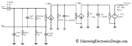
MasteringElectronicsDesign.com:Build an Op Amp SPICE Model from Its Datasheet – Part 1, Part 2, and Part 3 of this article show how to create a behavioral model of an operational amplifier based on the following parameters found in the datasheet: Input and output resistance, input capacitance, DC gain, offset voltage and gain bandwidth product. As an example I chose Analog Devices’ ADA4004 and built its behavioral model step by step. Figure 1 shows the model as we left off at the end of part 3.
Figure 1
Let’s continue building this model with some more parameters.
Input bias currents
The input bias currents flow in the op amp inputs to bias the input transistors. Ideally, these currents should be zero. (See my article MasteringElectronicsDesign.com:An Ideal Operational Amplifier Simulation Model.) This is not the case with real op amps. If the transistors in the input stage are bipolar, the base currents determine the op amp bias currents and they can be significant. If the input stage has JFET transistors, the bias currents are the gate leakage currents which are usually low, as in the case of our example ADA4004. The bias currents are the reason for which we always try to match the op amp input resistors. If the input resistors are not matched, the input bias currents create an input offset voltage due to the differential voltage drop on these resistors.
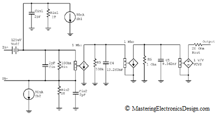
ADA4004 datasheet shows that the input bias currents are 40 nA typical and can be maximum 90 nA, at a power supply of +/-15 V and ambient temperature of 25 ºC. Let’s choose the worst case, which is 90 nA. To simulate the currents we will add two DC current sources between each input and ground, as in Figure 2. Let’s label them with Ib1 and Ib2.
Figure 2
Input Offset Current
The datasheet of any op amp also shows an offset current between the two inputs. This is the result of the difference between the input bias currents which are never identical. In fig 1 I connected two current sources between each input and ground, which are identical. In reality, this is rarely the case. There will always be a difference between the input bias currents, and this difference is the input offset current. For that reason, even with matched input resistors, there will always be a voltage offset due to the input offset currents. For high precision applications, one has to choose op amps with the lowest input offset current possible.
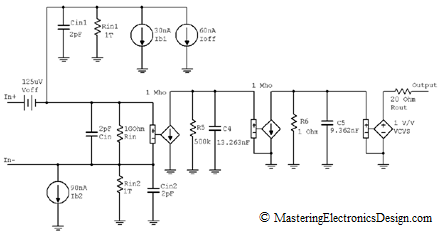
The datasheet shows that the offset current is maximum 60 nA at +/- 15 V and 25 ºC. To simulate the offset current, we will add an extra current source in parallel with one of the input current sources, say Ib1 (see fig 3). Let’s call it Ioff. It really it does not matter at which input we connect the offset current source, because the offset current can be positive or negative. What matters is the op amp output voltage deviation due to the offset current. Whether this deviation, construed as error, is positive or negative is of less importance.
Figure 3
If we add the offset current source at the non-inverting input, we need to subtract its value from Ib1. That way, the Op Amp non-inverting input bias current does not go over the specified value of 90 nA. Because of that, Figure 3 shows now Ib1 as being 30 nA.
With these last parameters, we built a fairly complex op amp macro model which can help us in any design with ADA4004. Similar builds can be done with other op amps, or specialized components like current sense circuits. The ideal components used in this 4-part article are generic, and can be found in any SPICE simulator.


At ADI, we test for 90 nA max on each input. Then we take the delta.
Your model would fail our final test program. It is 150/90.
You can use 90nA on one and 30nA on the other input. 90/30
or -85 and -26 and it would pass.
Harry Holt
PSG Applications
San Jose, CA
Harry.Holt@analog.com
Thank you, Harry, for your input. I corrected Figure 3.
Hi Adrian,
This is really helpful. I was just wondering if it will be possible to include the maximum output current and slew rate in the model.
Thanks
Sasha