I received a message from one of my readers asking me to help with a Wheatstone bridge circuit. Since my response to him bounced back, and this being an interesting subject, I decided to write this article. Here is what he writes:
“I found a circuit to condition the output of the Wheatstone bridge in the National ADC1205 datasheet, page 16. It uses an Op Amp configured as follows: V1 from the bridge thru 10K resistor to (–) input of Op Amp, 1.5Meg feedback resistor and Vout connects to the V- of the 5V ADC. V2 from the bridge connects directly to (+) input of the op amp and the V+ of the ADC.
The bridge V2-V1 is 0 mV to 30 mV. This is both at 5.000 V (0 mV) and V1 = 4.985 V, V2 = 5.015 V (30 mV). Please advise the equations to calculate how this works. Since the ADC is 5 V, I cannot see how the Vout can exceed that voltage. Is it true that Vout = 5.015 V when V1 = V2 = 5.015 V and ADC Out = 0 V?”
The National ADC1205 is an obsolete component now, but the advice and application notes are still valid. We can use any ADC if we can correctly adjust Vref and the operating conditions. We can use an Arduino board as well, with its 10-bit ADC to achieve a complete system.
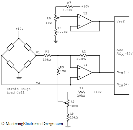
In Figure 1 I redrew the schematic to write my own notations on it.
Figure 1
The Op Amp U1 “rides” on top of V2. This means that Vout of LF412 will only “see” the difference between V1 and V2 times gain and plus V2. When V1 = V2 = 5 V, Vout will show V2 = 5 V.
When V1 increases by an amount dV = 15 mV as an example, and V2 decreases by the same amount, Vout will start descending from 5 V towards zero. Since the ADC samples the difference between V2 and Vout, its digital output will increase from zero towards Vref.
If V1 decreases by 15 mV and V2 increases by the same amount like my reader states, Vout start increasing above 5V, potentially going over the reference voltage and saturate the ADC. Therefore, I believe that the bridge should be wired such that V1 increases and V2 decreases when the bridge is unbalanced, like in the previous paragraph.
Vref needs to be adjusted to set the ADC full scale as we will see further. This is what the 1k potentiometer, R6, does. In the ADC1205 datasheet, R6 is labeled “gain”, but this is not correct. R6 is not the gain of the circuit. It simply sets Vref so that the ADC shows full scale when the bridge is fully loaded.
Vref depends on the 10V power supply and R6 wiper position. Its equation is as follows:
| |
(1) |
where with Vps I noted the power supply and with k1 the R6 percentage, between R6 wiper and R8.
When k1 is 100%, which means R6 wiper connected to R7, Vref is 5.29 V. When k1 is 0% (R6 wiper connected to R8) Vref is 3.86 V. Therefore, by adjusting the 1k resistor one can adjust the Full Scale ADC readout. One idea worth mentioning here is that the ADC full scale is
| |
(2) |
where with N I noted the ADC number of bits.
This means that the ADC full scale is not the reference voltage, but the reference voltage minus one LSB. For more information about this read my article An ADC and DAC Least Significant Bit (LSB).
The gain of the circuit is set by the ratio between R2 and R1. In this case, the gain is -150. When the bridge V1 and V2 voltage levels are changed in opposite direction by an amount of 15 mV, the total input signal in the amplifier is 30 mV. With a gain of 150, the full Vout swing is 4.5 V, which is inside the ADC 5 V range.
What about the potentiometer noted with R3?
(Continued on the next page.)


Hi,
How can we linearise the output of the bridge circuit?
It depends on how the bridge is built. If the sensor is one resistor in the bridge, the bridge output is non-linear. If the bridge is built such that two resistors on the same branch change by the same amount delta-R, one resistor increases by delta R and the other decreases by the same amount, the output is linear.
Hi,
I believe the statement ” The gain of the circuit is set by the ratio between R2 and R9″ is incorrect. The ratio should be between R2 and R1.
It was a typo. I corrected it. Thank you for your input.