Build an Op Amp SPICE Model from Its Datasheet – Part 2

Part 1 of this article (http://MasteringElectronicsDesign.com/buildi-an-op-amp-spice-model-from-its-datasheet/) shows how to create a behavioral model of an operational amplifier based on the following parameters found in the datasheet: Input and output resistance, input capacitance, DC gain, and offset voltage. As an example I chose Analog Devices’ ADA4004. Let’s continue building this model to simulate the Gain Bandwidth Product.

Gain Bandwidth Product

The Gain Bandwidth Product, describes the op amp behavior with frequency. Op amps have a dominant pole, inserted by manufacturers on purpose, so that the op amp is stable at any gain down to zero dB. See this article for more details: MasteringElectronicsDesign.com:An Op Amp Gain Bandwidth Product. In that article I showed that ADA4004 has a cutoff frequency at 24 Hz. This frequency is not identified in the datasheet, but can be easily calculated from the open-loop minimum gain of 500000 and the gain bandwidth product of 12 MHz.

Starting with the cut-off frequency, the open loop gain versus frequency plot has a drop of 20dB for every decade of frequency. To simulate this we need to introduce this pole in our SPICE model. Question is, how?

Read more

Build an Op Amp SPICE Model from Its Datasheet – Part 1

Why do you need to build your own Op Amp model? Most Op Amp manufacturers have SPICE models for their components and make them available for free. Then why should you know how to build one? Well, not everything has a model and that is why, sometimes, you have to build your own. Also, it may be necessary to study a circuit to see what happens if you change the Op Amp slew rate or bandwidth, offset, and so on. Sometimes the manufacturer own model does not work, as a user found out and posted a question in this forum. I told him that the model has a bug and advised him to build his own.

No matter the reason, building your own model is fun and rewarding and can only add to your overall understanding on how an Op Amp works. One note of caution. The model described here is a behavioral model. This means that the model will mimic the op amp functionality, but will not have any transistor or any other semiconductor SPICE models.

Read more

Using the Summing Amplifier as an Average Amplifier

Sometimes people ask how can one use a summing amplifier as an average amplifier. The answer is simple, provided that one knows what kind of average one needs.

The summing amplifier can output the average of two, three or more signals. This is different than a signal average. The summing amplifier cannot, for example, output the average of a triangle signal. For that, you need an integrator to perform the average in the analog realm, or you need to sample the signal and calculate the average with a microcontroller. This type of average is the signal average in the time domain. I will write an article about the average of a signal in a near future.

In this post I will show you how to average two or more signals with a summing amplifier. In How to Derive the Summing Amplifier Transfer Function I wrote that the summing amplifier shown in Figure 1

Read more

A Summing and Differential Amplifier with One Op Amp

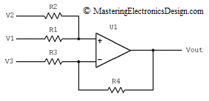
In a comment, one of my readers asked me what is the transfer function of the non-inverting summing amplifier in Figure 1, when R3 is connected to a reference voltage instead of ground.  Well, this is a summing amplifier with a differential configuration.

Figure 1

Read more

Design a Bipolar to Unipolar Converter with a 3-input Summing Amplifier

Since the publication of Design a Bipolar to Unipolar Converter to Drive an ADC, several readers contacted me with requests to help in solving their particular converter. The common problem they had was the fact that the components’ calculation resulted in a negative value for at least one resistor.

To provide a solution, first we need to understand the root cause of the problem. Let’s take one of the circuits I received and analyze it.

The reader wrote that he would like to drive an ADC with the input range of 0 to 2.5V from a signal with the range of –5V to +5V, connected at V1 (see Figure 1).

Read more

How to Design a Summing Amplifier Calculator

Several articles in this website describe the Summing Amplifier.  In one of these articles, Solving the Summing Amplifier, I showed a numeric method to design a non-inverting summing amplifier based on its input and output voltage range requirements.

This article shows how to design a summing amplifier calculator and the mathematical relations it uses.  You can find the calculator here:

JavaScript Summing Amplifier Calculator

Type the input voltage range, output range, a reference voltage and a choice of two resistors.  The calculator gives you the answer for the remaining two resistors.  The default values are for a bipolar to unipolar converter, which is explained in Design a Bipolar to Unipolar Converter to Drive an ADC.

What are the underlying equations?

Read more

Bipolar to Unipolar Converters Based on a Summing Amplifier Configuration

In a previous article, Design a Bipolar to Unipolar Converter to Drive an ADC, I presented a method for designing a bipolar to unipolar converter using a summing amplifier. In this article I am going to show more examples of bipolar to unipolar converters which are based on a summing amplifier configuration. You can adapt them to your needs if you use the method I described in the previous article.

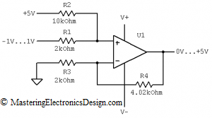
Input -1V to +1V, Output 0V to +5V, Reference voltage +5V

bipolar_to_unipolar_-1v_1v_to_0v_5v_1

Figure 1

Read more

Show Buttons
Hide Buttons
'