A differential amplifier frequent use is the amplification of the voltage difference between its inputs, while rejecting the common-mode level. However, the output common-mode level cannot be zero. The operational amplifier technological limitations, as well as the outside resistor tolerances let the common-mode voltage to make it to the amplifier output as an output error. As a consequence, the amplifier output voltage is the input signal difference times gain, plus the output common-mode voltage.
 Adrian S. Nastase
How to Design a Circuit from its Transfer Function Graph
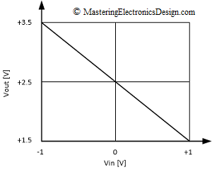
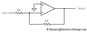
Sometimes all we know about a circuit is its transfer function graph. The transfer function might look like the one in Figure 1. How can we design a circuit so that its input-output behavior will match the graph?
The design starts with the mathematical form of the transfer function. This is a linear function, with the general form of a first order polynomial function.
Differential Amplifier Calculator
Unipolar to Bipolar Converter Example
If you need to design a differential amplifier, here is a handy calculator. All you need to define are the input range, the output range and a choice of voltage reference.
The differential amplifier was explained in different articles on this website. Solving the Differential Amplifier – Part 1, Part 2 and Part 3 shows a numerical example and how to design such an amplifier. Also, the common mode voltage level and the common mode output error were explained in the series of articles The Differential Amplifier Common-Mode Error – Part 1 and Part 2.
Enter the input range, Vin1 to Vin2, the output range, Vout1 to Vout2 and a reference voltage Vref. You need to choose two resistors, R2 and R3. The calculator will compute R1 and R4.
Design a Bipolar to Unipolar Converter with a 3-input Summing Amplifier
Since the publication of Design a Bipolar to Unipolar Converter to Drive an ADC, several readers contacted me with requests to help in solving their particular converter. The common problem they had was the fact that the components’ calculation resulted in a negative value for at least one resistor.
To provide a solution, first we need to understand the root cause of the problem. Let’s take one of the circuits I received and analyze it.
The reader wrote that he would like to drive an ADC with the input range of 0 to 2.5V from a signal with the range of –5V to +5V, connected at V1 (see Figure 1).
Summing Amplifier Calculator
Bipolar to Unipolar Converter Example
The calculator solves the summing amplifier resistors based on the input and output voltage range requirements. It is a great tool to design a bipolar to unipolar converter, as an example and other circuits.
Enter the input range, Vin1 to Vin2, the output range, Vout1 to Vout2 and a reference voltage Vref which helps in adjusting the common-mode level of the amplifier. Since the 2-input summing amplifier has 4 resistors, you need to choose two resistors, R1 and R3, and calculate R2 and R4. For more details about this calculator read How to Design a Summing Amplifier Calculator.
How to Design a Summing Amplifier Calculator
Several articles in this website describe the Summing Amplifier. In one of these articles, Solving the Summing Amplifier, I showed a numeric method to design a non-inverting summing amplifier based on its input and output voltage range requirements.
This article shows how to design a summing amplifier calculator and the mathematical relations it uses. You can find the calculator here:
JavaScript Summing Amplifier Calculator
Type the input voltage range, output range, a reference voltage and a choice of two resistors. The calculator gives you the answer for the remaining two resistors. The default values are for a bipolar to unipolar converter, which is explained in Design a Bipolar to Unipolar Converter to Drive an ADC.
What are the underlying equations?
The Virtual Ground
In my articles I talked about the op amp virtual ground and sometimes I wrote a brief explanation of this concept. In this article I will show you why an op amp input can be considered at a zero potential, without being galvanically connected to ground. Let’s take a simple circuit, the inverting amplifier.
In MasteringElectronicsDesign.com : How to Derive the Inverting Amplifier Transfer Function I showed the proof of its formula by using the virtual ground. The inverting input is at a zero potential, therefore virtual ground, which is a direct consequence of the feedback provided by R2 and the op amp high gain. Let’s see why.


