How to Derive the Differential Amplifier Transfer Function

The transfer function of the differential amplifier, also known as difference amplifier, can be found in articles, websites, formula tables, but where is it coming from? Why is the differential amplifier transfer function as in the following mathematical relation?

image0022 (1)

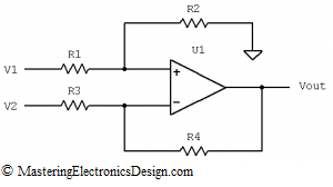
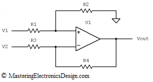
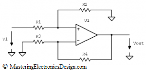
where the resistors are those shown in Figure 1.

differential_amplifier_1Figure 1

First, an important remark: This formula applies only for an ideal operational amplifier. This means that the amplifier has a large gain, so large that it can be considered infinity, and the input offset sufficiently small, so that it can be considered zero. Also, the input bias currents are sufficiently small so that they can be considered zero. I was once asked “but what is sufficiently small?” A voltage or current in electronics is considered sufficiently small, when its numerical value is 1/100 or less versus the dominant voltages or currents in the circuit. For example, if the input voltage levels, in the circuit in Figure 1, are around a few volts, and the operational amplifier input offset is millivolts or sub-millivolts, then we can neglect the input offset and consider it zero.

Having said that, do we need to know this formula by heart? Of course not. All we need to know is how to derive it. This is not difficult at all.

The transfer function can be derived with the help of the Superposition Theorem. This theorem says that the effect of all sources in a linear circuit is the algebraic sum of all of the effects of each source taken separately, in the same circuit. In other words (back at Figure 1), if we remove V1, and replace it with a short circuit to ground and calculate the output voltage, and then we do the same with V2, the output voltage of the differential amplifier is the sum of both output voltages as they were calculated with each source separately.

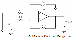
Let’s first remove V1. R1 cannot be left unconnected, because in the initial circuit there was current flowing through it.  Therefore, let’s ground R1 (see Figure 2).

differential_amplifier_21Figure 2

We can see that our amplifier becomes an inverter, which has its non-inverting input connected to ground through R1 and R2.  Vout2 is given in equation (2).

image008 (2)

Read MasteringElectronicsDesign.com: How to Derive the Inverting Amplifier Transfer Function for a proof of this function.

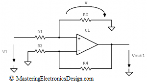
Now let’s remove V2 and ground R3 (see Figure 3).

differential_amplifier_3Figure 3

This is a non-inverting amplifier. For an ideal operational amplifier, Vout1 is a function of V, which is the voltage referred to ground at the non-inverting input of the operational amplifier.

image014 (3)

The resistors R1 and R2 are an attenuator for V1, so that V can be determined as in the following relation.

image016 (4)

By replacing V in equation (3), Vout1 becomes:

image018 (5)

Now that we have Vout1 and Vout2, and using the Superposition Theorem, Vout is the algebraic sum of Vout1 and Vout2,

image0201 (6)

which is the differential amplifier transfer function.  (Q.E.D.)

Solving the Differential Amplifier – Part 3

Design a Differential Amplifier by Inspection

Designing the differential amplifier by inspection is part of the art in the analog design.  Inspecting the circuit and knowing how it works, it really gives you a feeling on what the values of the resistors should be.

Looking back at the example I took in MasteringElectronicsDesign.com: Solving the Differential Amplifier – Part 1 and Part 2, we need to have an output signal of -1.25V to +2.365V with an input signal of -0.5V to 5.5V.  In those two articles I used the differential amplifier transfer function and I applied math to find the resistors.

This time I am going to demonstrate how this circuit can be solved by simple reasoning and knowing how it works. Some calculations are also necessary.  Cannot get rid of math totally.

Let’s write down the design requirements.

If Vin1 = -0.5V, then Vout1 = -1.25V and
If Vin2 = 5.5V, then Vout2 = 2.365V.

First, let’s remark the following:   If we bring a positive signal in the V1 input, the output will swing towards the positive rail.  If we connect a positive signal to V2, the output will swing towards the negative rail.  Of course, if the input signal is negative, the effect is opposite (see Figure 1).

differential_amplifier_1

Figure 1

The transfer function of the differential amplifier is as follows:

image004 (1)

For this function proof read MasteringElectronicsDesign.com: How to Derive the Differential Amplifier Transfer Function.

We will use V1 as the signal input, because the amplifier is not an inverter.   The design requirements show that, when the input swings positive, the output goes positive as well.  Let’s ignore for the moment V2. We will make V2 zero, by connecting R3 to ground (see Figure 2).  If V2 is zero the transfer function can be rewritten as in the following equation.

image007 (2)

differential_amplifier_2

Figure 2

The amplifier output in Figure 2 has to swing between -1.25V to +2.365V which means that the output total trip is

image009 (3)

The same can be written about the input range

image0101 (4)

Therefore the gain has to be

image0112 (5)

In effect, this circuit is an attenuator, with a sub-unity gain.

By comparing equations (2) and (5), we conclude that

image012 (6)

However, even if we do calculate the resistors based on equation (6), we know that there is something missing.  Although the output range of 3.615V is correct for the input range of 6V, when the input is at Vin1 voltage level, the output is not at Vout1.  By the same token, when Vin is at Vin2 level, the output is not Vout2.  Although the total trip at the amplifier output is correct, the extremities are not in the right position.  We need to introduce an offset, to move Vout1 in position, at -1.25V.  If we do that, since the swing is correct, Vout2 will fall at the correct voltage level of 2.365V.

How do we calculate the offset? If we multiply Vin1 with the amplifier gain, the result is

image0131 (7)

The difference between -0.301V and Vout2 = -1.25V is -0.949V.   This is the negative offset we need to introduce at the amplifier output. How do we do that? Enters V2.  A positive value at V2, will move the output in the opposite direction.  Comparing equations (1) and (2), the output offset is

image0141 (8)

We can choose for V2 any suitable voltage level or reference we have in our system.  If this is V2 = 2.5V, and after choosing a standard value for R3 = 10 kOhm, we can calculate R4 as 3.795 kOhm.  A standard value for R4 is 3.83 kOhm, with 1% tolerance.

Now that we know the resistor ratio R4/R3, R1/R2 can be easily calculated using equation (6).  After calculations, R1/R2 = 1.29.  Then we can choose R1 = 10 kOhm, therefore R2 = 7.754 kOhm.  A standard value for R2 is 7.68 kOhm, with 1% tolerance.

>>> <<<

Solving the Differential Amplifier – Part 2

Design a Differential Amplifier with the Coefficients Identification Method

In the first part of this series, MasteringElectronicsDesign.com: Solving the Differential Amplifier – Part 1, I wrote that the common usage of the differential amplifier is as a gain circuit for the differential voltage at its inputs.  When the circuit in Figure 1 has the resistor ratios equal

image001 (1)

the amplifier transfer function is

image002 (2)

and the circuit amplifies the difference between the input signals.

differential_amplifier_1

Figure 1

But the resistors’ calculation  becomes a bit of a challenge, when one might be faced with designing a differential amplifier with a certain transfer function.  The example I took in the first article was as follows:  Given an input range of, -0.5V to 5.5V, the output has to swing between, -1.25V and +2.365V.  I solved the problem by using the amplifier transfer function and a system of equations.

In this article I am going to write about designing the resistors of this differential amplifier using the method of coefficients identification.

Starting from the differential amplifier transfer function,

image004 (3)

we note that this is a linear function Vo, with two variables:  V1 and V2.  However, if we consider one of these two variables a known value, say, V2, Vo becomes a simple linear function with one variable.  Let’s note this function with Vo(V1).

The design requirements are as follows:

If Vin1 = -0.5V, then Vout1 = -1.25V and
If Vin2 = 5.5V, then Vout2 = 2.365V,

where by Vin1 and Vin2 I noted the input range limits, and by Vout1 and Vout2 I noted the output range limits.

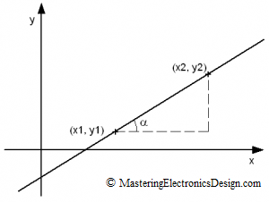
A linear function of first degree is a straight line which is determined by two points in the (x,y) plane (see Figure 2).

Linear Function

Figure 2

If we know one point (x1,y1) and the second point (x2,y2), we can determine the slope of the line, which is the tangent of the angle α between the x2-x1 and the hypotenuse of the triangle formed by the segments x2-x1 and y2-y1.

image010 (4)

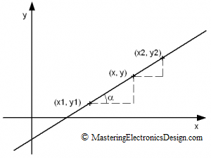
If we take an arbitrary point on this line between (x1,y1) and (x2,y2) and call it (x,y), the slope of the line has to be the same between the segment to the left and the one to the right of (x,y) point (see Figure 3).

image0111 (5)

linear_function_2

Figure 3

Solving for y in equation (5), the result the well known linear function y(x), that we know it goes through the first point (x1,y1) and the second point (x2,y2).

image013 (6)

Having said that, now we can compare the differential amplifier transfer function (3) with the linear function (6).  When these two functions are identical, Vo(V1) is y(x) and V1 is the variable x.  These are two linear functions that can be identical only if they have the coefficients identical, hence the name of the method.

image014 (7)

As y(x) is determined by its two points in plan, so is Vo(V1).  The given data points (Vin1, Vo1) and (Vin2, Vo2) determine the transfer function Vo(V1).  Therefore, (7) can be rewritten as the following system of equations.

image015 (8)

After replacing the known values Vin1, Vin2, Vout1 and Vout2 and after calculations, the system becomes

image016 (9)

which is exactly the result we had in part one of this series.

The system of equations (9) can be solved in the same manner as in the first article.   In brief, we choose the voltage reference V2, based on the available voltage references we have in the system, then we calculate the ratio .  Knowing this ratio we can calculate.  Then, knowing the resistor ratios, by choosing a pair of resistors say, R1 and R3 we can calculate R2 and R4.

Therefore, if we choose V2 = 2.5V, R3 = 10 kOhm, and R1 = 10 kOhm, the result is R4 = 3.795 kOhm, or a standard value of 3.83 kOhm, with 1% tolerance.  Also, R2 = 7.754 kOhm, or a standard value of 7.68 kOhm, with 1% tolerance.

Injecting AC into the DC Power Supply Rail

In allaboutcircuits.com forum, a question was posted: How can I combine an AC source of known frequency and amplitude with a DC power supply?

I thought this is an interesting problem, so here is the solution.

Subsequent messages clarified the requirements: 5V power supply, and the load needs 0.5A, which would make the load 10 ohms. The signal that rides on top of the DC voltage has to be 20 mVpkpk.

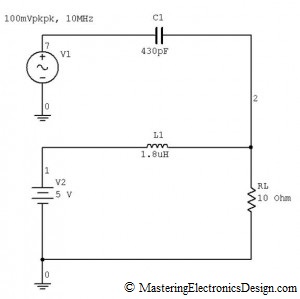
First, we need an inductor in series with the power supply to block the AC component. In this schematic, V1 is the 10 MHz generator and V2 is the 5V power supply.

image090426_1

The inductor’s impedance should be at least 10 times higher than the load, so that most of the generator energy goes into the load. If we note XL the inductor impedance, then XL = 10·RL,  so XL = 100 ohms, and L1 can be calculated

img2375

The result is L1 = 1.59 uH, with a standard value of 1.8 uH.

Then, we need a capacitor in series with the generator, to block the DC component from coming into the generator output. The generator, through this capacitor, “sees” the load in parallel with the inductor, considering that the power supply output impedance is low, close to zero.  Because of that, the capacitor impedance, together with the parallel combination load and inductor impedance form an attenuator. The signal amplitude on the load, can be written as follows:

img23821

where VL is the AC signal amplitude on load, VG is the generator amplitude, RLparXL is the load and inductor in parallel

img2377

and XC is the capacitor impedance. Using the above relation the capacitor impedance becomes

img2384

Taking into consideration that VL = 20 mVpkpk, L = 1.8 uH and choosing the generator amplitude VG = 100 mVpkpk, C1 becomes

img2394

with the result C1 = 433.07 pF. A standard value for C1 is 430 pF.

The generator amplitude can be slightly adjusted around 100 mVpkpk, so that the signal on load is exactly 20 mVpkpk.

And what is the current the generator sources on load? This can be easily calculated noting that the generator “sees” a capacitor in series with RL in parallel with L1. Since XC + RLparXL = 45.94 ohms, the generator output current is 2.18 mApkpk.

A 0.5 A, 1.8 uH inductor can be easily found. The generator sends into the power supply approximately 0.2 mApkpk signal. If this is not desirable, the inductor value can be increased with the disadvantage that its size increases.

Note that this method considers the load as being pure resistive. If the load has reactive components, RL has to be replaced by the combined impedance values of the resistive and reactive components.

Solving the Differential Amplifier – Part 1

Design a Differential Amplifier Based on the Input and Output Voltage Level Requirements

The differential amplifier, also known as the difference amplifier, is a universal linear processing circuit in the analog domain.  Why?  Because you can achieve any linear transfer function with it.  It can be reduced to a simple inverter, a voltage follower or a gain circuit.  It can also be transformed in a summing amplifier.

differential_amplifier_1

Figure 1

So, what is the common usage of the differential amplifier in Figure 1?  When the resistor ratios are equal

image001

the amplifier transfer function is

image002

and the circuit amplifies the difference between the input signals.

However, there are times when the electronics designer is faced with the following design requirements:  Given an input range of, say, -0.5V to 5.5V, the output has to swing between, say -1.25V and +2.365V.  It is clear that this requires an amplifier with a certain gain and an offset different than zero.  How can we design the differential amplifier to achieve such a function?

Read more

Why this website?

After many years of engineering in electronics design, I decided it is time to start a website with my views about this art.  Analog and mixed-signal design is not black magic or cryptology.  This is art, real and powerful and relevant.

The purpose of this website is to provide elegant solutions to analog and mixed-signal design problems that have a strong basis in math.  This website is not about Electronics in general.  This website is about the art form of designing electronic circuits.   My goal is to show hobbyists, engineering students and engineers that analog design is not complicated, so long as one understands the fundamentals and the reasoning behind the many aspects of the design.  Hopefully, if they see what a wonderful art electronics design is, more will be encouraged to pursue it.

As in Mathematics, where some solutions to problems are regarded as elegant, in Electronics one can enjoy the same treat, that fuzzy warm feeling of achievement, after a circuit is designed and works as expected.

Math is a central tool, for this website, which I use to prove a circuit or path of reasoning.  I disagree with articles, commentaries and books that take pride in the fact that they show a concept with no math involved.  In those cases students are invited to learn formulas by heart without any understanding of underlying physics, or where the formulas came from.  This deprives students of a powerful reasoning tool.

In the last decades, computer aided circuit design tools created a path of ease in electronics.  More and more people today apply a SPICE based program and then, when the prototype is built, wonder why it does not work.  In my view, SPICE should be used as a proofing tool after an engineer designed every aspect of his or her circuit.

To prove this alternate method of design, I will use SPICE and math at the same time.  I hope that I will start a conversation about electronics design where people can exchange ideas or get some help.

They say that analog and mixed-signal design engineers are in demand these days.  This is due to students’ reluctance to tackle analog design because it is too complicated, or because it involves too much Math and Physics.  I would like to change that.  Analog design is not complicated.  Analog design as well as mixed-signal design relies on Physics, from the knowledge one gets in high-school about electricity, to Maxwell’s equations.

Why analog and not digital design?  Well, there’s nothing wrong with digital design.  After all, everything today is digital, isn’t it?  Not quite.  The world, as we know it, is analog and the interface between the digital processing circuits and the outside world is handled by analog processing circuits.  In a lot of applications, the fine specifications or the secret sauce are handled by the analog circuitry.  For example, it is very important on how one chooses an analog to digital converter (“ADC”), and how the signal is shaped before the ADC.  Therefore, for all these reasons, this website puts more emphasis on analog circuitry rather than digital design.

Another outcome I am hoping to achieve is that youngsters will see that math is not difficult or abstract or useless.  Math is a tool like any other for real life designs, whether they are in Electronics, Physics, or Mechanics.  During my years of teaching Electronics at a university and calculus to my daughter, I really enjoyed the “aha” look on my students’ face, when they really got it, when their circuit worked, or when they solved a math problem.  Students are always eager to learn.  They only need someone to show the path.

Show Buttons
Hide Buttons
'