Why is the Op Amp Gain-Bandwidth Product Constant?

A recurring conversation I have usually starts with two questions: Why is the op amp gain-bandwidth product constant? And, how can we prove that?

The questions refer to the gain-bandwidth product behavior of an op amp after the cutoff frequency. As I showed in this article, MasteringElectronicsDesign.com: An Op Amp Gain Bandwidth Product, the gain bandwidth product describes the op amp gain dependency on frequency. The open loop graph is shown in Figure 1.

Read more

Apply Thevenin’s Theorem to Solve a Negative Resistance Circuit, or Current Source

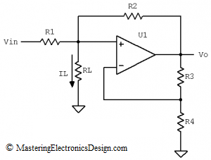
The circuit in Figure 1 is a good example of applying Thevenin’s Theorem to solve a circuit with dependent supplies. It is a negative resistance circuit and it was posted in this forum with a call for solution verification for IL as a function of Vin. With some clever resistor values, the circuit can also be a current source with RL its load. Since this fits very well with my plans to write more about Thevenin’s Theorem, I decided to post the solution here.

negative-resistance-circuit

Figure 1

Read more

An Op Amp Gain Bandwidth Product

I can see some chat on internet about the operational amplifier gain bandwidth product. People are interested in having a better understanding of this parameter, as it appears in any op amp datasheet and it is used in many articles and books. In this article I will describe this parameter and show you an example with Analog Devices’ ADA4004, which is a precision amplifier.

The Gain Bandwidth Product describes the op amp gain behavior with frequency. Manufacturers insert a dominant pole in the op amp frequency response, so that the output voltage versus frequency is predictable. Why do they do that? Because the operational amplifier, which is grown on a silicon die, has many active components, each one with its own cutoff frequency and frequency response. Because of that, the operational amplifier frequency response would be random, with poles and zeros which would differ from op amp to op amp even in the same family. As a consequence, manufacturers thought of introducing a dominant pole in the schematic, so that the op amp response becomes more predictable. It is a way of “standardizing” the op amp frequency response. At the same time, it makes the op amp more user friendly, because its stability in a schematic becomes more predictable.

Read more

The Virtual Ground

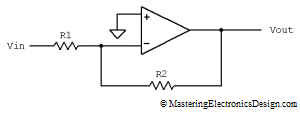
In my articles I talked about the op amp virtual ground and sometimes I wrote a brief explanation of this concept. In this article I will show you why an op amp input can be considered at a zero potential, without being galvanically connected to ground. Let’s take a simple circuit, the inverting amplifier.

inverting_amplifier_1Figure 1

In MasteringElectronicsDesign.com : How to Derive the Inverting Amplifier Transfer Function I showed the proof of its formula by using the virtual ground. The inverting input is at a zero potential, therefore virtual ground, which is a direct consequence of the feedback provided by R2 and the op amp high gain. Let’s see why.

Read more

The Non-Inverting Amplifier Output Resistance

It is customary to consider the output resistance of the non-inverting amplifier as being zero, but why is that? An Op Amp’s own output resistance is in the range of tens of ohms. Still, when we connect the Op Amp in a feedback configuration, the output resistance decreases dramatically. Why?

To answer these questions, let’s calculate the output resistance of the non-inverting amplifier.

It is widely accepted that the output resistance of a device can be calculated using a theoretical test voltage source connected at the device output. The input, or inputs, are connected to ground. Nevertheless, instead of using this method, let’s try a different one: The small signal variation method.

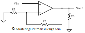
Figure 1 shows the non-inverting amplifier, which drives a load, RL. This circuit has an equivalent Thevenin source as in Figure 2.

non_inverting_amplifier

Figure 1

Read more

Show Buttons
Hide Buttons
'