Since the publication of Design a Bipolar to Unipolar Converter to Drive an ADC, several readers contacted me with requests to help in solving their particular converter. The common problem they had was the fact that the components’ calculation resulted in a negative value for at least one resistor.
To provide a solution, first we need to understand the root cause of the problem. Let’s take one of the circuits I received and analyze it.
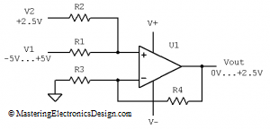
The reader wrote that he would like to drive an ADC with the input range of 0 to 2.5V from a signal with the range of –5V to +5V, connected at V1 (see Figure 1).
The reference voltage he had was 2.5V, connected at V2. After applying the method described in Design a Bipolar to Unipolar Converter to Drive an ADC, the result is that R4 is negative. Why is that?
A negative resistor means that the circuit needs a voltage source in order to comply with the output versus input requirements. This is because of the input range which is larger than the output range. In effect, the summing amplifier used for this circuit needs to be an attenuator. However, the non-inverting summing amplifier cannot be an attenuator, since it is a derivation from the non-inverting amplifier, which always has a gain greater than one. This conflict determines the negative resistor result.
There are two solutions to this problem: One is to reduce the reference voltage, V2, and another is to use a 3 input non-inverting summing amplifier.
I explained the first method in this article, How to Design a Summing Amplifier Calculator. Essentially, one needs to decrease the reference voltage to bring R4 into the positive realm. Read that article for more details.
Let’s talk about the second method. We will use a 3-input non-inverting summing amplifier to avoid resistor negative values when the input range is larger than the output range.
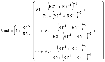
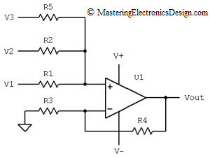
The multiple input non-inverting summing amplifier is explained in The Transfer Function of the Non-Inverting Summing Amplifier with “N” Input Signals. I wrote that article to show that, although some people avoid this amplifier due to its somewhat complicated transfer function, the derivation of the amplifier equation is not complicated. In that article, I also showed and explained the 3-input summing amplifier (see Figure 2). Its transfer function is as follows:
 |
(1) |
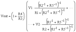
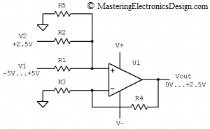
To design our elusive bipolar to unipolar converter, let’s connect the third input, resistor R5, to ground. The rest of the circuit is the same as in the case of the 2-input summing amplifier. If R5 is connected to ground, the V3 term in equation (1) disappears. The new transfer function is given in equation (2), and the schematic is shown in Figure 3.
 |
(2) |
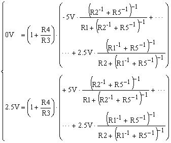
Now, it is clear what R5 does. It reduces the weigh of both V1 and V2. In effect, it attenuates both signals. With one extra resistor, the bipolar to unipolar amplifier is easier to be managed. Therefore, to do so, let’s write two equations, one for each end of the input signal trip.
 |
(3) |
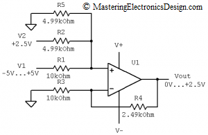
Next we choose R1 = 10 kOhms, R3 = 10 kOhms, R5 = 4.99 kOhms, and then we have to solve this system of two equations with 2 unknowns, R2 and R4.
If you have a math program like Mathcad, you can solve this system easily. If you don’t, you need to do it by hand. This is not an impossible task. Here are some hints.
We can take advantage of the fact that the two equations are products. Each unknown is part of each product term. Therefore, if we divide the first equation by the second, R4 disappears, and we have one equation with one unknown, R2. After we find R2, R4 can be easily derived by replacing R2 in the second equation.
The result is as follows:
R1 = 10kOhms, R2 = 4.99 kOhms, R3 = 10 kOhms, R4 = 2.49 kOhms, R5 = 4.99 kOhms.
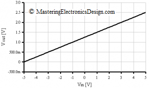
The final schematic is shown in Figure 4, and the transfer function graph in Figure 5.
>>> <<<




with this method, can you help me to design a formula so that it will view the actual value of the Vin
Use the bipolar to unipolar calculator
https://masteringelectronicsdesign.com/summing-amplifier-calculator-java/
to view the Vin value.
I have two questions, and both my math and my circuit analysis skills are rusty, so please forgive me.
Firstly, in your example you chose to fix R1, R3 and R5 to leave two unknowns for your two equations. How do you decide which Rx values you can fix, and which two you will solve for? I tried choosing different values and got non-sense results when I tried to solve…again, rough algebra skills at this point.
Secondly, if you choose R1 = 10k, is the V1 input impedance 10k? If the positive input on the op amp was being driven to zero I would be comfortable in saying this, but I am not sure what is happening in this case…again, rough circuit skills.
1. I chose R1, R3 and R5 so that the system of equations is easy to solve. As you noticed, the remaining unknowns are R4 and R2, each one in its own product term. So, If we divide one equation to another, R4 disappears and we get one equation with one unknown, R2.
2. No. If you look into the circuit from V1 point of view, you will notice that V1 “sees” R1 in series with R2 in parallel with R5. So the input impedance from V1 point of view is R1 + (R2 || R5).
Hi Adrian,
Thank you for great post. I’ve written the equations for this note for running in Microsoft Mathematics and I’m posting them here in case someone doesn’t want to retype them:
solve({(1+R_4/R_3)((-5)((R_2^-1+R_5^-1)^-1/(R_1+(R_2^-1+R_5^-1)^-1))+2.5((R_1^-1+R_5^-1)^-1/(R_2+(R_1^-1+R_5^-1)^-1)))=0,(1+R_4/R_3)((5)((R_2^-1+R_5^-1)^-1/(R_1+(R_2^-1+R_5^-1)^-1))+2.5((R_1^-1+R_5^-1)^-1/(R_2+(R_1^-1+R_5^-1)^-1)))=2.5,R_1=10,R_3=10,R_5=4.99})
Great. Thanks.