Design a Differential Amplifier by Inspection
Designing the differential amplifier by inspection is part of the art in the analog design. Inspecting the circuit and knowing how it works, it really gives you a feeling on what the values of the resistors should be.
Looking back at the example I took in MasteringElectronicsDesign.com: Solving the Differential Amplifier – Part 1 and Part 2, we need to have an output signal of -1.25V to +2.365V with an input signal of -0.5V to 5.5V. In those two articles I used the differential amplifier transfer function and I applied math to find the resistors.
This time I am going to demonstrate how this circuit can be solved by simple reasoning and knowing how it works. Some calculations are also necessary. Cannot get rid of math totally.
Let’s write down the design requirements.
If Vin1 = -0.5V, then Vout1 = -1.25V and
If Vin2 = 5.5V, then Vout2 = 2.365V.
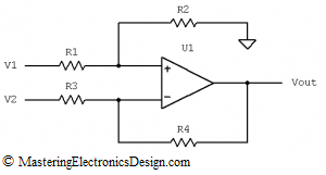
First, let’s remark the following: If we bring a positive signal in the V1 input, the output will swing towards the positive rail. If we connect a positive signal to V2, the output will swing towards the negative rail. Of course, if the input signal is negative, the effect is opposite (see Figure 1).
Figure 1
The transfer function of the differential amplifier is as follows:
| (1) |
For this function proof read MasteringElectronicsDesign.com: How to Derive the Differential Amplifier Transfer Function.
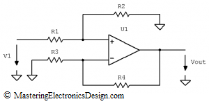
We will use V1 as the signal input, because the amplifier is not an inverter. The design requirements show that, when the input swings positive, the output goes positive as well. Let’s ignore for the moment V2. We will make V2 zero, by connecting R3 to ground (see Figure 2). If V2 is zero the transfer function can be rewritten as in the following equation.
| (2) |
Figure 2
The amplifier output in Figure 2 has to swing between -1.25V to +2.365V which means that the output total trip is
| (3) |
The same can be written about the input range
| (4) |
Therefore the gain has to be
| (5) |
In effect, this circuit is an attenuator, with a sub-unity gain.
By comparing equations (2) and (5), we conclude that
| (6) |
However, even if we do calculate the resistors based on equation (6), we know that there is something missing. Although the output range of 3.615V is correct for the input range of 6V, when the input is at Vin1 voltage level, the output is not at Vout1. By the same token, when Vin is at Vin2 level, the output is not Vout2. Although the total trip at the amplifier output is correct, the extremities are not in the right position. We need to introduce an offset, to move Vout1 in position, at -1.25V. If we do that, since the swing is correct, Vout2 will fall at the correct voltage level of 2.365V.
How do we calculate the offset? If we multiply Vin1 with the amplifier gain, the result is
| (7) |
The difference between -0.301V and Vout2 = -1.25V is -0.949V. This is the negative offset we need to introduce at the amplifier output. How do we do that? Enters V2. A positive value at V2, will move the output in the opposite direction. Comparing equations (1) and (2), the output offset is
| (8) |
We can choose for V2 any suitable voltage level or reference we have in our system. If this is V2 = 2.5V, and after choosing a standard value for R3 = 10 kOhm, we can calculate R4 as 3.795 kOhm. A standard value for R4 is 3.83 kOhm, with 1% tolerance.
Now that we know the resistor ratio R4/R3, R1/R2 can be easily calculated using equation (6). After calculations, R1/R2 = 1.29. Then we can choose R1 = 10 kOhm, therefore R2 = 7.754 kOhm. A standard value for R2 is 7.68 kOhm, with 1% tolerance.
>>> <<<


