An Op Amp Gain Bandwidth Product

I can see some chat on internet about the operational amplifier gain bandwidth product. People are interested in having a better understanding of this parameter, as it appears in any op amp datasheet and it is used in many articles and books. In this article I will describe this parameter and show you an example with Analog Devices’ ADA4004, which is a precision amplifier.

The Gain Bandwidth Product describes the op amp gain behavior with frequency. Manufacturers insert a dominant pole in the op amp frequency response, so that the output voltage versus frequency is predictable. Why do they do that? Because the operational amplifier, which is grown on a silicon die, has many active components, each one with its own cutoff frequency and frequency response. Because of that, the operational amplifier frequency response would be random, with poles and zeros which would differ from op amp to op amp even in the same family. As a consequence, manufacturers thought of introducing a dominant pole in the schematic, so that the op amp response becomes more predictable. It is a way of “standardizing” the op amp frequency response. At the same time, it makes the op amp more user friendly, because its stability in a schematic becomes more predictable.

Read more

Build an Op Amp SPICE Model from Its Datasheet – Part 1

Why do you need to build your own Op Amp model? Most Op Amp manufacturers have SPICE models for their components and make them available for free. Then why should you know how to build one? Well, not everything has a model and that is why, sometimes, you have to build your own. Also, it may be necessary to study a circuit to see what happens if you change the Op Amp slew rate or bandwidth, offset, and so on. Sometimes the manufacturer own model does not work, as a user found out and posted a question in this forum. I told him that the model has a bug and advised him to build his own.

No matter the reason, building your own model is fun and rewarding and can only add to your overall understanding on how an Op Amp works. One note of caution. The model described here is a behavioral model. This means that the model will mimic the op amp functionality, but will not have any transistor or any other semiconductor SPICE models.

Read more

An Ideal Operational Amplifier Simulation Model

You worked hard on your schematic, you calculated everything, you feel confident that it will work.  To be sure though, before committing the schematic to copper, you want to simulate it.  You develop a SPICE simulation schematic and, surprise, things don’t work.  What’s going on?

You start searching for bad connections in the simulation schematic.  You check the power supplies and the circuit biasing.  Finally, in desperation, you suspect the operational amplifier model that you downloaded from the manufacturer website, or found in the SPICE program library.  How do you troubleshoot your circuit?

First, split your circuit into small subcircuits, like a one op amp circuit.  Second, take aside, on a different simulation page, one of these subcircuits.  Is that working?  If that circuit is a non-inverting amplifier, as an example (Figure 1), and the output voltage is all over the place except your expected value, than replace your op amp with an ideal one and see if that circuit works.

Read more

A Summing and Differential Amplifier with One Op Amp

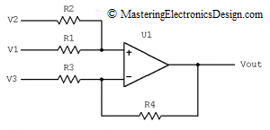
In a comment, one of my readers asked me what is the transfer function of the non-inverting summing amplifier in Figure 1, when R3 is connected to a reference voltage instead of ground.  Well, this is a summing amplifier with a differential configuration.

Figure 1

Read more

Differential Amplifier Output Common-Mode Voltage Calculator

A differential amplifier frequent use is the amplification of the voltage difference between its inputs, while rejecting the common-mode level.  However, the output common-mode level cannot be zero.  The operational amplifier technological limitations, as well as the outside resistor tolerances let the common-mode voltage to make it to the amplifier output as an output error.  As a consequence, the amplifier output voltage is the input signal difference times gain, plus the output common-mode voltage.

Read more

How to Design a Circuit from its Transfer Function Graph

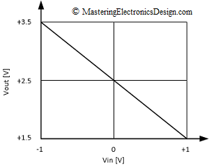
Sometimes all we know about a circuit is its transfer function graph.   The transfer function might look like the one in Figure 1.  How can we design a circuit so that its input-output behavior will match the graph?

Figure 1

The design starts with the mathematical form of the transfer function.  This is a linear function, with the general form of a first order polynomial function.

Read more

Design a Bipolar to Unipolar Converter with a 3-input Summing Amplifier

Since the publication of Design a Bipolar to Unipolar Converter to Drive an ADC, several readers contacted me with requests to help in solving their particular converter. The common problem they had was the fact that the components’ calculation resulted in a negative value for at least one resistor.

To provide a solution, first we need to understand the root cause of the problem. Let’s take one of the circuits I received and analyze it.

The reader wrote that he would like to drive an ADC with the input range of 0 to 2.5V from a signal with the range of –5V to +5V, connected at V1 (see Figure 1).

Read more

Show Buttons
Hide Buttons
'