Part 1 of this article (http://MasteringElectronicsDesign.com/buildi-an-op-amp-spice-model-from-its-datasheet/) shows how to create a behavioral model of an operational amplifier based on the following parameters found in the datasheet: Input and output resistance, input capacitance, DC gain, and offset voltage. As an example I chose Analog Devices’ ADA4004. Let’s continue building this model to simulate the Gain Bandwidth Product.
Gain Bandwidth Product
The Gain Bandwidth Product, describes the op amp behavior with frequency. Op amps have a dominant pole, inserted by manufacturers on purpose, so that the op amp is stable at any gain down to zero dB. See this article for more details: MasteringElectronicsDesign.com:An Op Amp Gain Bandwidth Product. In that article I showed that ADA4004 has a cutoff frequency at 24 Hz. This frequency is not identified in the datasheet, but can be easily calculated from the open-loop minimum gain of 500000 and the gain bandwidth product of 12 MHz.
Starting with the cut-off frequency, the open loop gain versus frequency plot has a drop of 20dB for every decade of frequency. To simulate this we need to introduce this pole in our SPICE model. Question is, how?
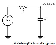
We could introduce a pole as in the following figure. This circuit shows a simple RC network with its cutoff frequency at 1/(2 π RC).
Figure 1
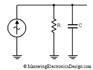
However, I prefer its Norton equivalent as in Figure 2.
Figure 2
My opinion is that it is easier to work with Norton sources, especially when one builds such pole and zero circuits. As with any current source, the frequency response depends on the load impedance. If we take an ideal current source generator with infinite bandwidth and load it with a resistor in parallel with a capacitor, the frequency response will be exactly one pole response.
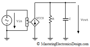
The circuit in Figure 3 shows a voltage controlled current source (VCCS) connected at a resistor-capacitor parallel network. Its input is driven by a voltage AC generator.
Figure 3
The transfer function of the current source has A/V = Mho units, so this is a transconductance amplifier. The circuit shown in Figure 3 has the following transfer function.
 |
(1) |
where with VCCS I noted the voltage-controlled-voltage-source transfer function which has units of Mho, and ω is the function variable.
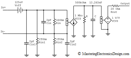
This transfer function can be adapted for ADA4004 if we choose the VCCS gain as 1 Mho, the resistor R = 500 kOhm and the capacitor C = 13.263 nF. The product between 1 Mho and 500 kOhm gives us the op amp gain of 500000 and the RC time constant sets the cutoff frequency at 24 Hz.
With this in mind, we can go back to our op amp model and replace the voltage-controlled-voltage-source (VCVS) with VCCS. However, we run into a problem. How do we isolate the RC network from our output resistor? If we simply replace the VCVS with the VCCS circuitry we just discussed, the output resistor and the op amp load will appear in parallel with the RC network, affecting our pole. The answer is simple. Add another VCVS with the transfer function of 1V/V.
The following figure shows the new ADA4004 model with all the elements we discussed until now.
Figure 4
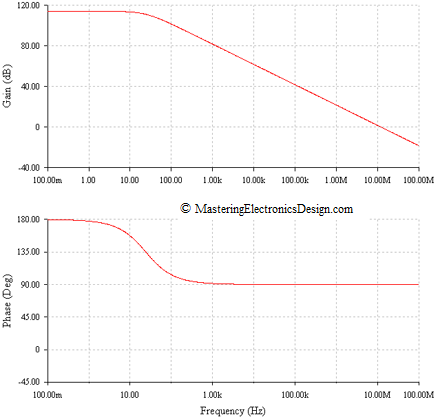
A Multisim simulation of the op amp open loop response is shown in Figure 5.
Figure 5
This Bode plot resembles ADA4004 open-loop gain characteristic as shown in its datasheet (Rev. F) Figure 14. However, there is a difference between my model’s Bode plot and the one shown in the datasheet. In the datasheet graph the phase starts to drop after 1 MHz. This means that there is another pole exactly where the phase becomes 45 degrees. We will see in the next article how to include that pole in the model.




I would like to thank you for the efforts you have put in writing this web site. I am hoping the same high-grade blog post from you in the upcoming as well. Actually your creative writing abilities has encouraged me to get my own blog now. Actually the blogging is spreading its wings rapidly. Your write up is a good example of it.
Thank you, Whitney.
I think you mean to say the cut off frequency is 24 Hz not 24 MHz.
Yes. Thank you for seeing that typo. I corrected it.
Sir,why the opamp output level is shifted by variying the duty cycle?
I do not have any signal with a duty-cycle in this article. If you want me to help you need to tell me what article/schematic/figure you are taking about. Or, if this is a general question, let me know in what context.
How do I model the maximum output voltage?
Place a positive power supply and a negative power supply at the op amp output. Connect a diode with the anode at the output and cathode at the positive supply. Connect another diode with the cathode at the output and the anode at the negative supply. The positive power supply value has to be the maximum op amp’s output trip plus 0.6V (a diode drop) and the negative supply value has to be the minimum op amp’s output trip minus a diode drop.
Thank you Adrian. And also, appreciate the work you’ve done.
I like this
Hello Adrian,
Thanks a lot for posting this detailed example of Op-Amp. It was really helpful.
Just one question though, how can we setup the supply voltage Vsy = +/-15V in this circuit i.e. V+ & V- in ADA4004-1 model ? I tried to connect the photodiodes b/w V+ & output and V- and output as suggested by you previously in comments. But this reduces the V(out) OR output Gain by a magnitude of order of 1000.
If I understood correctly, that’s how we setup the V+/V- OR in general terms the Vcc+/Vcc- power supply nodes?
Thanks a lot.
Saurabh Bedi.
How did you get the transfer function you did?
Why wouldn’t the single pole Transfer function be R/(RC*jw+1) ?
For the simple voltage source and RC circuit the transfer function would be 1/(RC*jw+1)
That is correct. I had a typo, now corrected. Thank you for seeing it.