The Instrumentation Amplifier (IA) resembles the differential amplifier, with the main difference that the inputs are buffered by two Op Amps. Besides that, it is designed for low DC offset, low offset drift with temperature, low input bias currents and high common-mode rejection ratio. These qualities make the IA very useful in analog circuit design, in precision applications and in sensor signal processing.
Figure 1
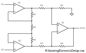
Figure 1 shows one of the most common configurations of the instrumentation amplifier. Its clever design allows U1 and U2 operational amplifiers to share the current through the feedback resistors R5, R6 and RG. Because of that, one single resistor change, RG, changes the instrumentation amplifier gain, as we will see further. RG is called the “gain resistor”. If the amplifier is integrated on a single monolithic chip, RG is usually left outside so that the user can change the gain as he wishes. One example of such instrumentation amplifier is Texas Instruments’ INA128/INA129.
To minimize the common-mode error and increase the CMRR (Common-Mode Rejection Ratio), the differential amplifier resistor ratios R2/R1 and R4/R3 are equal. (See The Differential Amplifier Common-Mode Error Part 1 and Part 2 for more on this matter.)
Another potential error generator is the input bias current. Although, in most analysis, the input current into an Op Amp is considered zero, in reality that is not the case. A small input current flows into the Op Amp inputs and is converted into voltage by the input resistors. If the resistors are not equal, the voltage difference between the two generates an offset, which is amplified and transmitted at the circuit output. Because of that, R1 is designed to be equal with R3. Similarly, R2 equals R4.
How do we derive the instrumentation amplifier transfer function?
It is well known that the instrumentation amplifier transfer function in Figure 1 is
| (1) |
when R5 = R6, R2 = R4 and R1 = R3.
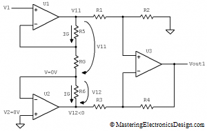
The proof of this transfer function starts with the Superposition Theorem. Let’s make V2 zero by connecting the U2 input to ground, and let’s calculate Vout1 (see Figure 2).
Figure 2
The calculation of Vout1 starts from the differential amplifier transfer function shown in equation (2). U3 is in a differential configuration. If we note the voltage levels at U1 and U2 outputs with V11 and V12 respectively, Vout1 can be written as
| (2) |
For the proof of equation (2) see The Differential Amplifier Transfer Function on this website.
To determine V11 and V12 we note that, if V2 is zero, the node between RG and R6 is a virtual ground. This is because U2 sets its output at such a level, so that its inverting input equals the non-inverting input potential. With this observation, one would realize that U1 is in a non-inverting amplifier configuration, with its feedback resistor network R5 and RG connected to a virtual ground.
Therefore, V11 can be deduced from the non-inverting amplifier transfer function:
| (3) |
In order to calculate V12, let’s observe that the current that flows through R5 and RG, IG, is the same as the current through R6. That is because there is no other current path. The currents that flow into U1 and U2 inputs are too small to be taken into consideration. Mathematically, we can write that the current through R5 and RG equals the current through R6 as in equation (4). Since the node between RG and R6 is at zero volts, V11 appears as a voltage drop on R5 and RG in series. Also, V12 is the voltage drop on R6, forcing the output of U2 to be driven below ground.
| (4) |
Therefore, V12 is
| (5) |
Replacing V11 and V12 in equation (2), Vout1 becomes
| (6) |
After calculations, and taking into consideration that R5 = R6, the result for Vout1 is as in equation (7).
| (7) |
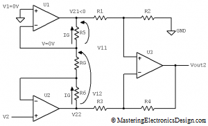
For the second part of the Superposition Theorem, let’s restore V2 and let’s make V1 zero. We will note the output voltage with Vout2, and with V21 and V22 the output voltage of U1 and U2 respectively (see Figure 3).
Figure 3
Vout2 depends on V21 and V22 in a similar manner as Vout1 in equation (2).
| (8) |
This time, U2 is in a non-inverting configuration, so that V22 can be written as a function of V2 as in (9).
| (9) |
The circuit is symmetric, so we can write a similar equation for V21 and V22 as equation (4) for V11 and V12.
| (10) |
and therefore, V21 is
| (11) |
Replacing V21 and V22 in equation (8) and after calculations, we find Vout2 as in the following expression.
| (12) |
All we need to do now is to add Vout1 and Vout2 to find the instrumentation amplifier transfer function. The result is given in equation (13).
| (13) |
Q. E. D.
>>> <<<
If we take a closer look at the instrumentation amplifier transfer function, we note that, if RG is not connected and R2 = R1, the circuit gain becomes one. Changing one single resistor, RG, results in large gain variations, so it gives the analog designer flexibility in his application. This is the reason why the IC manufacturers choose not to integrate RG on the monolithic chip, and also choose to make R1, R2, R3 and R4 equal. As opposed to the differential amplifier, where the user has to change at least two resistors to change the gain, in instrumentation amplifiers one resistor does the job, bringing elegance and simplicity in the analog design.


you did not solve equation number 6.how did u obtain equation 7 after solving equation 6
Arun, here are the calculations:
First, factorize V1*(1+R5/RG),
Vout1 = (R2/R1)*(V1*(1+R5/RG)*(1+R6/(R5+RG)))
Then, introduce 1 in each fraction,
Vout1 = (R2/R1)*(V1*(RG+R5)/RG*(R5+RG+R6)/(R5+RG))
Simplify RG+R5
Vout1 = (R2/R1)*V1*(R5+RG+R6)/RG
And, because R5=R6,
Vout1 = (R2/R1)*V1*(RG+2R5)/RG
Distribute RG, and this is the final result:
Vout1 = V1*(R2/R1)*(1+2R5/RG)
Let me know if you need anything else.
I looked at the derivation for the transfer function of the differential amplifier, as linked, but the transfer function proven on that page looks nothing like equation 2. How did you derive equation 2 of this page from the differential amplifier’s transfer function?
Grant, the two equations are identical, if R1 = R3 and R2 = R4 as stated two paragraphs above.
Equation (2) in this article is Vout1 = R2/R1 *(V11-V12).
Equation (1) in How to Derive the Differential Amplifier Transfer Function is Vout = V1 * R2/(R1+R2) * (1+R4/R3) – V2 * R4/R3.
If R1 = R3 and R2 = R4 then
R2/(R1+R2) * (1+R4/R3) = R2/(R1+R2) * (1+R2/R1) = R2/R1, and
R4/R3 = R2/R1
The inputs of the differential amplifier, which is the instrumentation amplifier output stage, are V11 instead of V1 and V12 instead of V2. We also note Vout with Vout1. Therefore, from the differential amplifier transfer function, as applied to the instrumentation amplifier output stage we get
Vout1 = V11 * R2/(R1+R2) * (1+R4/R3) – V12 * R4/R3 = V11 * R2/R1 – V12 * R2/R1 = R2/R1 * (V11 – V12),
exactly as shown in equation (2).
Thank you. I was looking at the same thing. This clarifies. Great article by the way.
Ley us U3 non inverting terminal voltage Vp then
Vp=V11*R2/(R1+R2). {by voltage divider rule}
& Inverting terminal is connected R3 with V12 voltage
Now. R4=R2,R3=R1,
Apply superposition theorem
(1). Vp=0 then U3 act like a inverting amplifier
So Vout(1)’= –(R4/R3)V12,=–(R2/R1)V12,
(2) V12=0 then U3 act like a non-inverting amplifier so, Vout(1)”=Vp*(1+R4/R3)=(1+R2/R1)Vp
=(1+R2/R1)(R2/R1+R2)*V11
Vout(1)” = V11*(R2/R1)
Vout1=Vout(1)’+Vout(1)”
=R2/R1*(V11–V12)
Hi,
If input voltages V1 and V2 are the same, does it mean that output voltage equals zero volt?
Yes, it will be zero. But nothing is a perfect zero in this Universe. You will still have a few millivolts at the amplifier output due to offset, or due to V1 and V2 not being perfectly equal.
Hi, if U3 is up side down, means R4 connects to ground and R2 connects to Vout and U3 has the opposite sign. Will all the equation be not changed?
for example, will the equation 2 become Vout1=R2/R1(V12-V11)?
Thank you
The notations are just a convention. Your U3 being turned upside down, is the same as saying “let’s call the upper transistors R3 and R4 and the lower transistors R1 and R2, and let’s switch V11 and V12 labels between them”. The resistor ratio is the same, since R4/R3 = R2/R1. Because we switched V11 and V12, then, yes, Vout1 = R2/R1 (V12-V11).
Adrian, In fig 2 applying KCL at node between Rg and R6, the current direction should be towards that node. Current should flow out from both opamps. Only then will equation 10 be valid, right?
No, not right. The current that flows from U1 output through R5 and RG is the same current that flows through R6 and into the output of U2. Current does not flow out from both Op Amps. If flows out from U1 and into U2 when V1 is greater than V2 as in figure 2. Equation 10 refers to figure 3 not 2. In figure 3, V2 is greater than V1 and current flows from U2 and into U1.
what is the significance of output voltage in the instrumentation amplifier?
As equation 13 shows, Vout is directly proportional with the difference between the amplifier two inputs.
how to design an instrumentation amplifier to get 2v output from 1 and 0mv input with designing step
I think my article shows that. You need to choose an instrumentation amplifier (go to digikey.com) and look in the data sheet for the transfer function. Should be similar with what I describe here. You need to calculate a resistor value to set the gain. 1 mV is a small signal. You need to choose a low noise amplifier with low offset.
How to decide the value of the resistor R1,R2,R3,R4,R5,R6 ?
What I know the value should be the same.
Is it if we put the too high or too small it will affect the gain ?
What is the best range value for the resistor, because my input is in mV from the Wheatstone Bridge.
and for the Vout VALUE, is it we need to evaluate by our own value to calculate the value of RG?
Look at the last paragraph of this article. Choose all resistors equal, with a value of 1kohm to 10kohm, and then calculate RG to give you the desired gain. The gain is shown in Eq 1.
I use 200kohm for every resistors. Is the value make sense ?
I am now in the process of designing signal conditioning circuit for thermistor.
The temperature range is between 0-100 deg C.
So I make the maximum temperature which is 100 deg C as maximum output voltage which is 5V.
The value for V1 measured is 131.35mV
the value for V2 measured is 27.41mV
Then I calculate using your equation by substitute the Vo as 5V
and I find the value of RG is about 8491ohm.
Is my calculation is correct or not ?
Hello.
Very helpful articles.
Im in the process of design my signal conditioning circuit for thermistor. I do need this amplifier since the output from Wheatstone Bridge is in mV.
Is it make sense the resistor I used for this amplifier is all 200k ohm ?
Is it too big ?
I would use 10kohm resistors.
How to drive common mode gain of the first stage?
I don’t understand this question. You need to reformulate it.
Prove that the gain of the INA 126 amplifier is equal to ? ?
?? ????/??
hello,how to design an intrumentations amplifers to satisfy a fixed differential voltage gain of Af=500? please reply me as soon as possible
You can use INA126 (Texas Instruments). RG is the gain resistor. With RG = 162 ohms, 1% tolerance, the gain is 500.