Why do you need to build your own Op Amp model? Most Op Amp manufacturers have SPICE models for their components and make them available for free. Then why should you know how to build one? Well, not everything has a model and that is why, sometimes, you have to build your own. Also, it may be necessary to study a circuit to see what happens if you change the Op Amp slew rate or bandwidth, offset, and so on. Sometimes the manufacturer own model does not work, as a user found out and posted a question in this forum. I told him that the model has a bug and advised him to build his own.
No matter the reason, building your own model is fun and rewarding and can only add to your overall understanding on how an Op Amp works. One note of caution. The model described here is a behavioral model. This means that the model will mimic the op amp functionality, but will not have any transistor or any other semiconductor SPICE models.
Setting the Gain
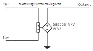
The simplest Op Amp model is a Voltage-Controlled-Voltage-Source (VCVS) (see my article MasteringElectronicsDesign.com:An Ideal Operational Amplifier Simulation Model). We can build the model around it. This VCVS also helps in setting the Op Amp open-loop gain.
Let’s take an example. Let’s build a model for the Analog Devices’ ADA4004, which is a precision operational amplifier. At the time this article was published, Analog Devices did not release a SPICE model for this op amp.
The datasheet shows that the open-loop gain, AVO, is minimum 500V/mV. This means a gain of 500000 at DC level, so my VCVS will have the transfer function of 500000 V/V. Let’s build this op amp model in Multisim (see Figure 1). (Note: Multisim is a simulation program with a SPICE engine. It was developed by Electronics Workbench and now owned by National Instruments. Check this link http://MasteringElectronicsDesign.com/spice-links/ for info where to find Multisim, and also other simulation programs.)
Figure 1
Input and Output Resistance
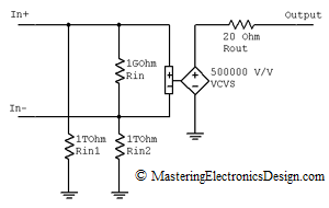
The input resistance can be defined in the datasheet of an op amp as a group of three resistors: Rin1, Rin2 and Rin. These resistors represent the input common-mode resistance on the non-inverting/inverting inputs and the differential input resistance. As such, in our Multisim model let’s add these resistors in the VCVS input as in Figure 2.
The ADA4004 does not have a specification for the input resistance. This is most likely due to the fact that ADA4004 is made with the Analog Devices’ new iPolar technology which is an enhanced JFET technology. As such, the input resistance is very high, up to 1012 ohms. Let’s estimate the common-mode resistance as 1012 ohms and the differential input resistance as 1 Gohm. Having these resistors in the model will not make too much of a difference, therefore the model will work very well with or without them for this particular op amp. However, other op amps, built with different technologies, will have lower input resistance values and they will make a difference in the SPICE model.
The output resistance is not specified as well for this op amp. Because of that we will estimate a 20 ohm series resistor with the op amp output. Let’s add it as in figure 2.
Figure 2
The Input Capacitance
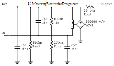
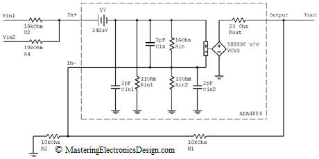
As in the case with the input resistance, the input capacitance of an op amp can be specified as three input capacitors, Cin1, Cin2 and Cin. They represent the input common-mode capacitance on the non-inverting/inverting inputs and the differential input capacitance. Let’s add them in parallel with the input resistors, as in Figure 3.
The ADA4004 does not have these capacitances specified in the datasheet. Because of that, let’s make them a conservative value of 2 pF each.
Figure 3
The Offset Voltage
If we power an op amp with a bipolar power supply and connect the inputs to ground, the output will not go to zero volts. It will likely rail up or down due to the offset voltage. This voltage is present in any op amp at its inputs. The output rails up because the op amp high gain, multiplied by the input offset voltage, makes a theoretical voltage of tens of volts, so the output will be limited by the available power supply level.
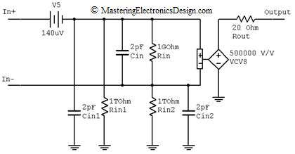
To simulate this voltage, all we have to do is add a DC voltage source in series with one of the inputs, say the non-inverting input, as in Figure 4. The ADA4004 offset voltage is typical 40μV, maximum 140μV. We can choose the typical value for our model, but we can also choose the worst-case value, of 140μV, as in the figure, if we want to study the op amp behavior in these conditions.
Figure 4
This model can now be connected in a circuit. Figure 5 shows a non-inverting summing amplifier made with our ADA4004 model.
Figure 5
In the next article I will show you how to add the gain bandwidth product and how to add poles in this model. We will also see that it is better to use Voltage-Controlled-Current-Sources (VCCS) to build the op amp SPICE model than the VCVSs.




Adrian this is a great resource! Op Amps are used in many circuits and I am always a bit perplexed by how they work in the circuit.
Thank you Mark. Nice to see you dropped by.
I can see how this model forces the input voltage from IN+ to IN- to near zero volts.
If you were to reverse the IN+ and IN- connection on a real opamp then the summing function would not work?
AppsMan, no it would not work. You need to preserve the negative feedback and this can only be done by using IN- for the feedback resistor. If you need an inverting summing amplifier, read this article How to Derive the Transfer Function of the Inverting Summing Amplifier.
Hi,
This is Srihari, i went through your article, its a fantastic source and inspiration for people like me get started.
I have this query, i need your help on this
Objective: Fully differential precision amplifier modeling
Given data: Open loop gain – 90db, small signal bw(200mV p-p) – 118Mhz,
THD+Noise 3Vpp@1Khz, HD2 = -124.7db, HD3 = -139.9dB
Also other parameters are also provided, like Gain BW product = 200MHz
As per the understanding
90db = 31623 gain
BW = GBP/open loop gain = 200Mhz/31623 = 6.324kHz cutoff freq
Therefore with gm=1Mho R=31.623k C=1/2piRC = 0.8nF
First order model is developed, but to get small signal bw of 118MHz i scalled C to 1.342nF because 200M/118M = 1.69 so 1.69*0.8nF = 1.342nF
Now a VCVS at the output with Gain of 1 will give the desired result for dominant pole, bw etc. If we are to introduce THD, HD2, HD3 we need to introduce noise at VCVS with some coefficient.
Can you please help me how to model this THD, HD2, HD3 in spice.
Thanks
Srihari
Srihari, THD and Harmonics cannot be modeled with a behavioral method. You need to recreate the Op Amp with non-linear elements like transistors and diodes. They are the source of distortions. That is why semiconductor companies release SPICE models for their components, because the Op Amp design engineers intimately know the component schematic and the process through which the Op Amp is grown on the silicon wafer. With a macro model as described in this article one can do as much, to accurately test a DC schematic and some AC behavior. Each model has its limitations, and that is why one has to understand the underlying physics and know how much he can trust the model.
I’m glad you find this article useful. Thank you for visiting.
Very nicely done. There are vendors who’ll give you a SPICE model and vendors who’ll only give you the datasheet (or maybe something IBIS). So for those vendor parts with slight holes in their support offerings, this will come very much in handy.
It wasn’t that long ago that we had to go through the whole process of building a similar model for a transformer, complete with all the parasitics, so we feel for you. In our case, though, the model was somewhat simpler (at least as was required in our application) but the datasheets even sketchier. And before we were done, we were measuring values with an LRC meter that that magnetics manufacturer was either unwilling or unable to publish.
Thank you Eric for your input. That’s exactly why I wrote this series.
All the opamp datasheets that I’ve checked have no parameters for input common mode or differential resistance. Is there a way to derive these parameters from the input bias current, input offset voltage, or other datasheet parameters that are typically provided?
Actually, many op amp datasheets have the input resistance specified. It depends on the manufacturer. Take a look at Analog Devices amplifiers. Here are some examples, ADA4896, ADA4528, ADA4891, ADA4898, ADA4051, ADA4062, ADA4075, just to mention a few. However, if the input resistance is missing, I would divide the specified maximum input common mode voltage to the bias current to get the common mode resistance, ballpark number. With that, you can estimate the differential input resistance, by dividing the common mode resistance by 10…100.
How to adjust that the op amp has VCC and – VCC as maximum output voltage
Place a diode between output and +Vcc with the anode connected to output. Also, place a diode between -Vcc and output with the anode connected to -Vcc.