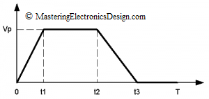
In this article I will show you how to calculate the RMS value of a trapezoidal waveform. This periodic waveform is shown in Figure 1. It has a rise time from 0 to t1 and a fall time from t2 to t3. The plateau is between t1 and t2, and the signal is periodic with the period T. If you know this, then you can derive the RMS value of a triangle, square and pulse waveform as well. Go to How to Derive the RMS Value of a Triangle Waveform and How to Derive the RMS Value of Pulse and Square Waveforms for further reading.
Analog Design
An ADC and DAC Least Significant Bit (LSB)
Articles on Internet and books show how to calculate the Least Significant Bit (LSB), but they take into consideration either the voltage reference (Vref) or the full scale (FS) of the ADC or DAC. Many times this leads to confusion, as a few messages I received from my readers show. Therefore, this article shows both ways of defining the LSB, so that people will have a clear understanding how to treat an ADC’s (Analog-to-Digital-Converter) or DAC’s (Digital-to-Analog-Converter) LSB.
Differential Amplifier Output Common-Mode Voltage Calculator
A differential amplifier frequent use is the amplification of the voltage difference between its inputs, while rejecting the common-mode level. However, the output common-mode level cannot be zero. The operational amplifier technological limitations, as well as the outside resistor tolerances let the common-mode voltage to make it to the amplifier output as an output error. As a consequence, the amplifier output voltage is the input signal difference times gain, plus the output common-mode voltage.
How to Design a Circuit from its Transfer Function Graph
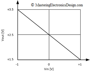
Sometimes all we know about a circuit is its transfer function graph. The transfer function might look like the one in Figure 1. How can we design a circuit so that its input-output behavior will match the graph?
The design starts with the mathematical form of the transfer function. This is a linear function, with the general form of a first order polynomial function.
Differential Amplifier Calculator
Unipolar to Bipolar Converter Example
If you need to design a differential amplifier, here is a handy calculator. All you need to define are the input range, the output range and a choice of voltage reference.
The differential amplifier was explained in different articles on this website. Solving the Differential Amplifier – Part 1, Part 2 and Part 3 shows a numerical example and how to design such an amplifier. Also, the common mode voltage level and the common mode output error were explained in the series of articles The Differential Amplifier Common-Mode Error – Part 1 and Part 2.
Enter the input range, Vin1 to Vin2, the output range, Vout1 to Vout2 and a reference voltage Vref. You need to choose two resistors, R2 and R3. The calculator will compute R1 and R4.
Design a Bipolar to Unipolar Converter with a 3-input Summing Amplifier
Since the publication of Design a Bipolar to Unipolar Converter to Drive an ADC, several readers contacted me with requests to help in solving their particular converter. The common problem they had was the fact that the components’ calculation resulted in a negative value for at least one resistor.
To provide a solution, first we need to understand the root cause of the problem. Let’s take one of the circuits I received and analyze it.
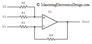
The reader wrote that he would like to drive an ADC with the input range of 0 to 2.5V from a signal with the range of –5V to +5V, connected at V1 (see Figure 1).


