Bipolar to Unipolar Converters Based on a Summing Amplifier Configuration

In a previous article, Design a Bipolar to Unipolar Converter to Drive an ADC, I presented a method for designing a bipolar to unipolar converter using a summing amplifier. In this article I am going to show more examples of bipolar to unipolar converters which are based on a summing amplifier configuration. You can adapt them to your needs if you use the method I described in the previous article.

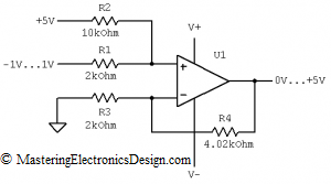
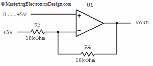
Input -1V to +1V, Output 0V to +5V, Reference voltage +5V

bipolar_to_unipolar_-1v_1v_to_0v_5v_1

Figure 1

Read more

Design a Differential Amplifier the Easy Way with Mathcad

For those of you who have Mathcad, designing a differential amplifier is really easy.

Let’s say you need to design a unipolar to bipolar converter and you decide to use a differential amplifier for this task. You know the input and output voltage range and you need to calculate the resistors based on a voltage reference you have in the system. All you have to do is to create a Mathcad file for a quick response. Then store it some place for future designs.

If you would like to know why the unipolar to bipolar converter can be designed with a differential amplifier, read this article, Design a Unipolar to Bipolar Converter for a Unipolar Voltage Output DAC .

Let’s take an example.

Read more

Design a Unipolar to Bipolar Converter for a Unipolar Voltage Output DAC

Unipolar to bipolar converters are useful when we have to have a unipolar component to do a certain job in a mixed signal design environment.  For example, Digital to Analog Converters (DACs) may have the output voltage range 0 to 2.5 V, or 0 to 5 V, while the design asks for a range of –5 V to +5 V.  To comply with this requirement, we have to design a unipolar to bipolar converter which will be inserted between the DAC output and the following bipolar stage.  It looks like the circuit in Figure 1.  How did I design it?

unipolar_to_bipolar_converter_1Figure 1

Read more

Design a Bipolar to Unipolar Converter to Drive an ADC

Most Analog to Digital Converters have a unipolar input that can be a problem when designing bipolar circuits.  Some common ADC input voltage ranges are 0 to 2.5 V, or 0 to 5 V.  However, the analog circuit that drives the ADC can have voltage swings of, –1 V to +1 V, –2 V to +2 V , –5 V to +5 V, and so on.  Bringing the ADC input below ground is a big No-No, because the current from input will flow through the chip substrate creating irreversible changes in the ADC and damage it.  So, how do we connect a bipolar front end circuit with a unipolar ADC?  Enters the bipolar to unipolar converter.  Let’s design one.

The converter can be designed with a summing amplifier, as in Figure 1.  How do we calculate the resistors?

summing_amplifier1

Figure 1

Read more

Differential Output Circuit

One of my readers asked me to explain how I designed a circuit I posted in a forum, as a solution to one of the member’s question.  The problem was about designing a circuit with 3 input signals, VA, VB and VCM.  The circuit had to output the sum and difference between VCM and the average of VA and VB as in the following expressions:

image0011 (1)

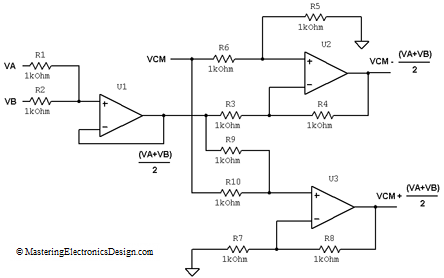
The solution I posted is the circuit in Figure 1.

differential_output_circuit

Figure 1

What is the easiest way to design this circuit?

Read more

The Transfer Function of an Amplifier with a Bridge in the Negative Feedback

In allaboutcircuits.com forum an interesting circuit was posted. The question was, how to determine the transfer function, Vout/Vin?

The circuit schematic was drawn as in Figure 1.

fig1

Figure 1

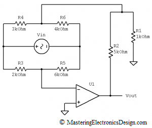
To make a point regarding its feedback and for clarity, I redrew it as in Figure 2.

fig2

Figure 2

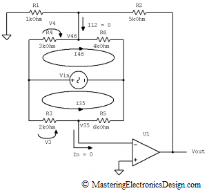
Now, things started to make more sense. R1 and R2 are feedback resistors. Also, the bridge does not alter the feedback, because there is no current going through it from Vout to the bridge and to U1 input. Assuming that U1 is close to an ideal amplifier, its bias current in the inverting input is zero. Therefore, whatever current emerges from the R1 and R2 node, noted with I12, and goes to the bridge is zero. Also, the current that goes into the inverting input, In, has to be zero.

It becomes clear now that the circuit is very simple. The only currents that Vin generates are local currents, I46 and I35, through the bridge legs.

Let’s write the voltage difference V46-V35, which is the voltage that alters Vout. I will call it Vbridge.

image003

This voltage alters Vout because it appears in the amplifier input. For that reason, Vout is given by the following equation:

image004 (1)

The amplifier output adjusts Vout so that V35 = 0V. The inverting input is at a virtual ground, so we can write Vbridge as

image005 (2)

If we find out V46 as a function of Vin, the circuit is solved. How do we calculate it?

By inspecting the bridge we can write V46 as follows:

image006 (3)

The current through R3 and R5 is I35 and its value can be written as in the following equation.

image007

With I35 known we can calculate V3.

image008

Following the same train of thoughts, V4 is

image009

By replacing V3 and V4 in (3), V46 in (2) and Vbridge in (1), the transfer function is

image010

Q.E.D. (quod erat demonstrandum)

>>>  <<<

This equation shows us that, if the bridge is balanced, when

image0111

the output voltage is zero. Hence, this circuit can be used for tuning, or for measurements, when one of the resistors in the bridge is a sensor. Due to the resistor ratios in the transfer function, the actual resistor value does not matter. What matters is the ratio of these resistors. As a consequence, the circuit is insensitive to temperature variations because, if all resistors are from the same technological process, the voltage at output does not change with temperature. If we choose a good operational amplifier, with a low temperature drift and low offset, this amplifier can be used in precision measurements.

Solving the Differential Amplifier – Part 2

Design a Differential Amplifier with the Coefficients Identification Method

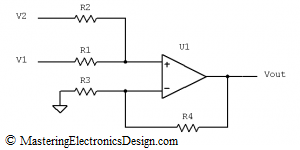
In the first part of this series, MasteringElectronicsDesign.com: Solving the Differential Amplifier – Part 1, I wrote that the common usage of the differential amplifier is as a gain circuit for the differential voltage at its inputs.  When the circuit in Figure 1 has the resistor ratios equal

image001 (1)

the amplifier transfer function is

image002 (2)

and the circuit amplifies the difference between the input signals.
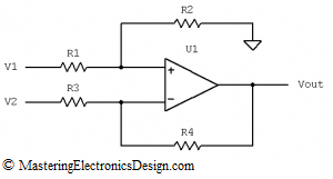
differential_amplifier_1

Figure 1

But the resistors’ calculation  becomes a bit of a challenge, when one might be faced with designing a differential amplifier with a certain transfer function.  The example I took in the first article was as follows:  Given an input range of, -0.5V to 5.5V, the output has to swing between, -1.25V and +2.365V.  I solved the problem by using the amplifier transfer function and a system of equations.

In this article I am going to write about designing the resistors of this differential amplifier using the method of coefficients identification.

Starting from the differential amplifier transfer function,

image004 (3)

we note that this is a linear function Vo, with two variables:  V1 and V2.  However, if we consider one of these two variables a known value, say, V2, Vo becomes a simple linear function with one variable.  Let’s note this function with Vo(V1).

The design requirements are as follows:

If Vin1 = -0.5V, then Vout1 = -1.25V and
If Vin2 = 5.5V, then Vout2 = 2.365V,

where by Vin1 and Vin2 I noted the input range limits, and by Vout1 and Vout2 I noted the output range limits.

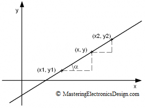
A linear function of first degree is a straight line which is determined by two points in the (x,y) plane (see Figure 2).
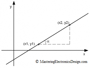
Linear Function

Figure 2

If we know one point (x1,y1) and the second point (x2,y2), we can determine the slope of the line, which is the tangent of the angle α between the x2-x1 and the hypotenuse of the triangle formed by the segments x2-x1 and y2-y1.

image010 (4)

If we take an arbitrary point on this line between (x1,y1) and (x2,y2) and call it (x,y), the slope of the line has to be the same between the segment to the left and the one to the right of (x,y) point (see Figure 3).

image0111 (5)

linear_function_2

Figure 3

Solving for y in equation (5), the result the well known linear function y(x), that we know it goes through the first point (x1,y1) and the second point (x2,y2).

image013 (6)

Having said that, now we can compare the differential amplifier transfer function (3) with the linear function (6).  When these two functions are identical, Vo(V1) is y(x) and V1 is the variable x.  These are two linear functions that can be identical only if they have the coefficients identical, hence the name of the method.

image014 (7)

As y(x) is determined by its two points in plan, so is Vo(V1).  The given data points (Vin1, Vo1) and (Vin2, Vo2) determine the transfer function Vo(V1).  Therefore, (7) can be rewritten as the following system of equations.

image015 (8)

After replacing the known values Vin1, Vin2, Vout1 and Vout2 and after calculations, the system becomes

image016 (9)

which is exactly the result we had in part one of this series.

The system of equations (9) can be solved in the same manner as in the first article.   In brief, we choose the voltage reference V2, based on the available voltage references we have in the system, then we calculate the ratio .  Knowing this ratio we can calculate.  Then, knowing the resistor ratios, by choosing a pair of resistors say, R1 and R3 we can calculate R2 and R4.

Therefore, if we choose V2 = 2.5V, R3 = 10 kOhm, and R1 = 10 kOhm, the result is R4 = 3.795 kOhm, or a standard value of 3.83 kOhm, with 1% tolerance.  Also, R2 = 7.754 kOhm, or a standard value of 7.68 kOhm, with 1% tolerance.

Show Buttons
Hide Buttons
'