Measure a Bipolar Signal with an Arduino Board

Arduino is a popular family of open source microcontroller boards. Hobbyists, students and engineers all over the world use this platform to quickly design and prototype a microcontroller driven circuit. One of its interfaces with the analog world is the ADC. Since these boards are mostly designed around an ATMEL ATmega32 or ATmega168 microcontroller, the ADC has 8 inputs and 10-bit resolution, making it suitable for many applications.

From time to time I receive a message through my Contact page with the question, how to interface a sensor, or an outside circuit with the Arduino ADC? In most cases the answer is an interface between a bipolar circuit and the Arduino board. As the bipolar circuit output varies from some negative to a positive level, the Arduino ADC cannot measure this signal directly, because the ADC inputs can only be between 0V and the reference voltage.

In one of these messages a reader asked me how to build an interface between a board that has an output voltage of -2.5V to +2.5V and the Arduino ADC. He told me that the Arduino reference voltage is AVCC = 5V. He would like to measure the +/-2.5V signal with the Arduino board and direct the microcontroller to take some action based on the result.

Read more

Measure a Wheatstone Bridge Sensor Signal with an ADC

I received a message from one of my readers asking me to help with a Wheatstone bridge circuit. Since my response to him bounced back, and this being an interesting subject, I decided to write this article. Here is what he writes:

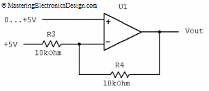
I found a circuit to condition the output of the Wheatstone bridge in the National ADC1205 datasheet, page 16. It uses an Op Amp configured as follows: V1 from the bridge thru 10K resistor to (–) input of Op Amp, 1.5Meg feedback resistor and Vout connects to the V- of the 5V ADC. V2 from the bridge connects directly to (+) input of the op amp and the V+ of the ADC.

The bridge V2-V1 is 0 mV to 30 mV. This is both at 5.000 V (0 mV) and V1 = 4.985 V, V2 = 5.015 V (30 mV). Please advise the equations to calculate how this works. Since the ADC is 5 V, I cannot see how the Vout can exceed that voltage. Is it true that Vout = 5.015 V when V1 = V2 = 5.015 V and ADC Out = 0 V?

The National ADC1205 is an obsolete component now, but the advice and application notes are still valid. We can use any ADC if we can correctly adjust Vref and the operating conditions. We can use an Arduino board as well, with its 10-bit ADC to achieve a complete system.

Read more

An ADC and DAC Least Significant Bit (LSB)

Articles on Internet and books show how to calculate the Least Significant Bit (LSB), but they take into consideration either the voltage reference (Vref) or the full scale (FS) of the ADC or DAC.  Many times this leads to confusion, as a few messages I received from my readers show.  Therefore, this article shows both ways of defining the LSB, so that people will have a clear understanding how to treat an ADC’s (Analog-to-Digital-Converter) or DAC’s (Digital-to-Analog-Converter) LSB.

Read more

Design a Unipolar to Bipolar Converter for a Unipolar Voltage Output DAC

Unipolar to bipolar converters are useful when we have to have a unipolar component to do a certain job in a mixed signal design environment.  For example, Digital to Analog Converters (DACs) may have the output voltage range 0 to 2.5 V, or 0 to 5 V, while the design asks for a range of –5 V to +5 V.  To comply with this requirement, we have to design a unipolar to bipolar converter which will be inserted between the DAC output and the following bipolar stage.  It looks like the circuit in Figure 1.  How did I design it?

unipolar_to_bipolar_converter_1Figure 1

Read more

Design a Bipolar to Unipolar Converter to Drive an ADC

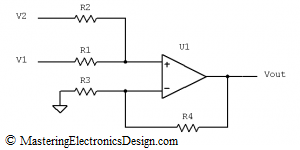
Most Analog to Digital Converters have a unipolar input that can be a problem when designing bipolar circuits.  Some common ADC input voltage ranges are 0 to 2.5 V, or 0 to 5 V.  However, the analog circuit that drives the ADC can have voltage swings of, –1 V to +1 V, –2 V to +2 V , –5 V to +5 V, and so on.  Bringing the ADC input below ground is a big No-No, because the current from input will flow through the chip substrate creating irreversible changes in the ADC and damage it.  So, how do we connect a bipolar front end circuit with a unipolar ADC?  Enters the bipolar to unipolar converter.  Let’s design one.

The converter can be designed with a summing amplifier, as in Figure 1.  How do we calculate the resistors?

summing_amplifier1

Figure 1

Read more

An ADC and DAC Differential Non-Linearity (DNL)

As in the case of INL, DNL is an important parameter of an ADC or DAC because it is a measure of their non-linearity.  DNL stands for Differential Non-Linearity and quantifies the ADC or DAC precision.

The term differential refers to the values an ADC takes between two consecutive levels.  When the input signal swings in any direction, the ADC samples the signal and its output is a stream of binary numbers.  An ideal ADC will step up or down one Least Significant Bit (LSB), without skipping any level and without holding the same decimal number past two or three LSBs. However, due to technological limitations, ADCs and even DACs are not ideal.  When that happens, the ADC’s linearity is severely impacted.  Therefore, DNL is defined as the maximum deviation from one LSB between two consecutive levels, over the entire transfer function.

In an electronic system, linearity is important.  When an ADC is non-linear, it brings imprecision in measurements.  If a DAC is non-linear, it restores a dynamic signal with high distortions.  Moreover, an accumulation of skipped levels, or high DNL, can increase the INL as well.

Figuring out the DNL value is quite simple. One has to measure the ADC response to a voltage value that would correspond to one LSB. For example, if we have a 12-bit ADC and the voltage reference is 2.5V, one LSB is given by the following equation.

image001

So, for each 0.6103 mV increase in the ADC input, the output hexadecimal value will increase with one.
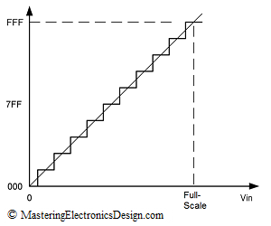
figure-1

Figure 1

An ideal ADC transfer function is shown in Figure 1.  This is a 12-bit ADC, but the steps are exaggerated for better viewing.  There is no deviation from 1 LSB step, so the DNL is zero.
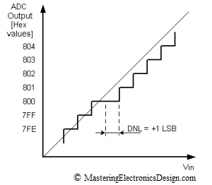
figure-2_2

Figure 2

In Figure 2, the ADC holds the 0x800 hex output for two full steps. Since the deviation is towards the positive values on the X scale, and the ADC output holds the same value for an extra LSB, the Differential Non-Linearity is +1 LSB.
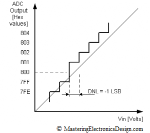
figure-2_3

Figure 3

Figure 3 shows that the DNL migrated towards negative values for one LSB. Therefore, DNL in Figure 3 is -1 LSB. Since 0x800 is missing, there the ADC is categorized with missing codes.  Such an ADC cannot be used for high precision applications.

The DNL in Figure 4 is -0.75, because the 0x800 is still there, but for a shorter voltage range than one LSB.  The code is still there, so the ADC can be used in precision applications.
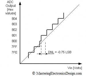
figure-3_2

Figure 4

In Figure 5, the 0x800 step appears at lower voltage inputs than one LSB.  The DNL is -1.25 LSB. It is clear that the ADC is highly non-linear.  Moreover, it is categorized non-monotonic.  High DNL values, positive or negative can increase the INL as well.
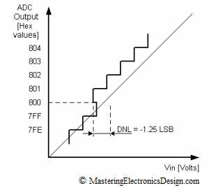
figure-2_4

Figure 5

A non-monotonic DAC is highly undesirable, especially if the DAC is used in a closed loop application like servo or process controls.  With a non-monotonic DAC the system may become unstable, or the control may suffer from jumpiness, jitteriness and overall difficult control handling.

The main rule for precision applications is to choose a component with a DNL less than one LSB. In this case, the ADC or DAC is assured monotonicity, no missing codes and a good linearity.

An ADC and DAC Integral Non-Linearity (INL)

What is INL?  This term describes the non-linearity of Analog to Digital Converters (ADC) and Digital to Analog Converters (DAC).  INL stands for Integral Non-Linearity.  Is this term important? Should we be concerned about this specification?  The answer is yes.

INL is considered an important parameter because it is a measure of an ADC or DAC non-linearity error.  However, as in any Analog or Mixed-Signal Design project, some specifications are important, some are not.  It all depends on the project requirements regarding accuracy and precision.  Understanding INL enables the circuit designer to avoid surprises in his or her project.

The Integral Non-Linearity is defined as the maximum deviation of the ADC transfer function from the best-fit line.  An ADC function is to digitize a signal into a stream of digital words called samples.  The ADC output is discrete as opposed to the input, which is continuous.  It is used at the boundary between the analog and digital realms.

The ADC input is usually connected to an operational amplifier, maybe a summing or a differential amplifier which are linear circuits and process an analog signal.  As the ADC is included in the signal chain, we would like the same linearity to be maintained at the ADC level as well.  However, inherent technological limitations make the ADC non-linear to some extent and this is where the INL comes into play.

figure-1

Figure 1

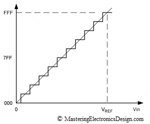
Figure 1 shows the ADC transfer function.  For each voltage in the ADC input there is a corresponding word at the ADC output.  The figure shows a 12-bit ADC where the steps were exaggerated for better viewing.  The y axis, the output, is digital, so that the values are represented in hexadecimal format.  If the ADC is ideal, the steps shown are perfectly superimposed on a line.

figure-2

Figure 2

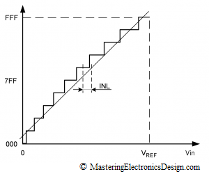
Figure 2 shows an ADC with a slight non-linearity.  To express the non-linearity in a standard way, manufacturers draw a line through the ADC transfer function, called the best fit line.  The maximum deviation from this line is called INL, which can be expressed in percentage of the full scale or in LSBs (List Significant Bit). INL is measured from the center of each step to that point on the line, where the center of the step would be if the ADC was ideal.

This parameter is important because it cannot be calibrated out.  The ADC non-linearity is unpredictable.  We don’t know where on the ADC scale the maximum deviation from the ideal line is.  Therefore, if one of the design requirements is good accuracy, we need to choose an ADC with the INL within the accuracy specifications, or a lot less than the specified error.

For example, let’s say the electronic device we design has an ADC that needs to measure the input signal with a precision of 0.5% of full-scale.  Due to the ADC quantization, if we choose a 12-bit ADC, the initial measurement error is +/- 1/2 LSB which is called the quantization error.

image0031

With the ADC quantization error almost 40 times lower than the design requirements, a 12-bit ADC can do a good job for us.  However, if the INL is large, the actual ADC error may come close to the design requirements of 0.5%.  We would like to keep each component error in the circuit as low as possible, so that the total combined error of the electronic device we design is less than 0.5%.  Gain or offset errors in an ADC can be calibrated out, but INL cannot.  If we need to live with an evil, at least we need to choose an ADC with a small INL.  This may increase the cost we allocate for the ADC in the system, but it is worthwhile if we are to keep our promises and design a device within specifications.

The DAC Integral Non-Linearity can be viewed the same as for an ADC.  The only difference is that, with a DAC, the INL may not be as important.  If the DAC is used to set a few voltage levels in a system, those values may be easily calibrated, so we can choose a low cost DAC.  However, if the DAC is used to accurately restore a dynamic signal, the INL cannot be easily calibrated.  In that case, we need to choose a high precision DAC, with a good INL.

Show Buttons
Hide Buttons
'