How to Design a Summing Amplifier Based on the Input and Output Voltage Level Requirements
In allaboutcircuits.com forum a member asked how can he drive a MOSFET that needs a voltage range of 4V to 5V with a DAC with the output range of 0V to 5V?
Initially I thought he should use a differential amplifier. However, based on the articles I published, MasteringElectronicsDesign.com: Solving the Differential Amplifier – Part 1, Part 2 and Part3 the solution based on a differential amplifier would require a negative voltage level in the input. Although V1 can be the input from 0V to 5V, V2 has to be negative, so that the output shifts to positive values.
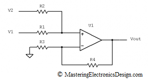
Then I thought of the Summing Amplifier, or the Non-Inverting Summing Amplifier, which is shown in Figure 1. It is called a summing amplifier, because two signals are summed in one of the amplifier inputs. In this case, V1 and V2 are summed in the non-inverting input.
The summing of V1 and V2 is not direct. Resistors R1 and R2 make a weighted sum and this is what makes this amplifier very useful. As in the case with the differential amplifier, one can use this circuit to achieve any linear function. This article shows you how to design a summing amplifier based on the input and output requirements. You can also solve your amplifier with the calculator I posted here: MasteringElectronicsDesign.com: Summing Amplifier Calculator.
The transfer function of the summing amplifier is as follows.
| (1) |
You can find its demonstration in this article, MasteringElectronicsDesign.com: How to Derive the Summing Amplifier Transfer Function.
Let’s write down what we know:
If Vin1 = 0V then Vout1 = 4V and
If Vin2 = 5V then Vout2 = 5V,
where by Vin1 and Vin2 I noted the input range limits, and by Vout1 and Vout2 I noted the output range limits.
Let’s choose one of the summing amplifier inputs to be Vin, say V1.
Because we have two instances that we know, Vin1 and Vin2 and the corresponding outputs, Vout1 and Vout2, let’s rewrite equation (1) using these two instances.
 |
(2) |
This is a linear system of two equations with a lot of unknowns: R1, R2, R3, R4 and V2. However, we can simplify our life by grouping the resistors in ratios. The equations can be rewritten like this,
 |
(3) |
where by k1 and k2 I noted:
 |
(4) |
Now we are left with three unknowns, k1, k2, V2. I can simply consider V2 as a known value, because I can connect to R2 any voltage I want or, more conveniently, a voltage that I already have in the circuit. I will target for V2 = 5V, since there is already a DAC in this circuit with an output range of 0 to 5V. So I can assume there is a 5V reference in this circuit.
If k1 and k2 are the remaining unknowns, then (3) is a system of two equations and two unknowns as in (5), which can be easily solved.
 |
(5) |
It can be easily seen that the second equation becomes
| (6) |
so k2 has to be zero.
The result is k1 = 1/4 and k2 = 0.
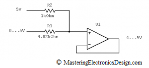
This result shows that we do not need the resistors R3 and R4. Also, the ratio between R2 and R1 is 1/4. We can choose R2 = 1 kohm and a standard value for R1 = 4.02 kohm with a 1% tolerance.
The final circuit is shown in Figure 2.
Since k2 is zero, R3 is zero, configuring U1 as a repeater for the summed voltage in the non inverting input.


That is clever! good job Analog guru!
Thank you, Laura.
I’ve being trying to solve this for a while, until I noticed your post. Now it looks so simple. Great post, by the way.
You posted the solution of a circuit in this forum,
http://www.edaboard.com/ftopic355461.html
and you said that you used this article and also Solving the Differential Amplifier part 1
https://masteringelectronicsdesign.com/solving-the-differential-amplifier-part-1/
I have trouble calculating the resistors. Can you please explain how you calculated that circuit?
Leonard, I will write a post with the calculations. Follow this blog. I will post the article soon.
=======================================
Update: You can find this article here: Differential Output Circuit.
Is the summing amplifier used as an error amplifier?
Yes, the summing amplifier is used as an error amplifier in many systems. For example, the non-inverting summing amplifier with two inputs has on one input the control signal and, on the other one, the inverted feedback. The weighted sum also gives the designer the opportunity to adjust the feedback versus the control signal. Moreover, dynamic compensations can be achieved easily. More on this subject in a future article.
Nice article.
But I didn’t get this part:
”
It can be easily seen that the second equation becomes
… (6)
”
How is it easy? I don’t see it.
“R1 = 1 kohm and a standard value for R2 = 4.02”
This should be R2 = 1kOhm and R1 = 4.02kOhm!
Here are the steps for equation (6);
Start with the second equation in system (5).
5V = (5V * k1/(1+k1) + 5V * 1/(1+k1)) * (1+k2)
Factorize 5V in the first parenthesis.
5V = 5V * (k1/(1+k1) + 1/(1+k1)) * (1+k2)
The two fractions have the same denominator, so they can be added into one fraction.
5V = 5V * (k1+1)/(1+k1)) * (1+k2)
Since the numerator and denominator are equal, the fraction is 1. The result is equation (6).
5V = 5V * (1+k2)
As for R1 and R2 values, thank you for pointing out the error. The calculations and figure are correct, but the values are inverted in the conclusion. I will correct that. Update: Corrected.
I am glad you liked the article. Thank you for visiting, and for thoroughly checking it.
Hi, I like your article very much and I can learn a lot from it.
But, I have a question. In your case, u set V2=5V, V1 is 0-5V (the output V range of DAC). what if V2 is a variable value? does this method still work? I mean I am going to connect V2 to a negative terminal of a solar cell, and the output voltage is variable due to a load.
How can I solve Vout with a Variable V2? many thanks.
You need to tell me more. I need the input range -x to +y, and the desired output range. The circuit needs to be recalculated for these conditions. In fact, what I think you are looking for is a bipolar to unipolar converter. You might want to read my article Design a Bipolar to Unipolar Converter to Drive an ADC.