How to Design a Summing Amplifier Calculator

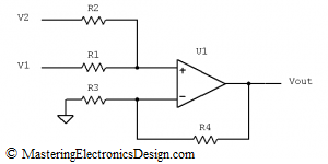
Several articles in this website describe the Summing Amplifier.  In one of these articles, Solving the Summing Amplifier, I showed a numeric method to design a non-inverting summing amplifier based on its input and output voltage range requirements.

This article shows how to design a summing amplifier calculator and the mathematical relations it uses.  You can find the calculator here:

JavaScript Summing Amplifier Calculator

Type the input voltage range, output range, a reference voltage and a choice of two resistors.  The calculator gives you the answer for the remaining two resistors.  The default values are for a bipolar to unipolar converter, which is explained in Design a Bipolar to Unipolar Converter to Drive an ADC.

What are the underlying equations?

Read more

The Virtual Ground

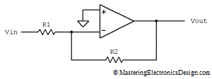
In my articles I talked about the op amp virtual ground and sometimes I wrote a brief explanation of this concept. In this article I will show you why an op amp input can be considered at a zero potential, without being galvanically connected to ground. Let’s take a simple circuit, the inverting amplifier.

inverting_amplifier_1Figure 1

In MasteringElectronicsDesign.com : How to Derive the Inverting Amplifier Transfer Function I showed the proof of its formula by using the virtual ground. The inverting input is at a zero potential, therefore virtual ground, which is a direct consequence of the feedback provided by R2 and the op amp high gain. Let’s see why.

Read more

Bipolar to Unipolar Converters Based on a Summing Amplifier Configuration

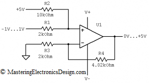
In a previous article, Design a Bipolar to Unipolar Converter to Drive an ADC, I presented a method for designing a bipolar to unipolar converter using a summing amplifier. In this article I am going to show more examples of bipolar to unipolar converters which are based on a summing amplifier configuration. You can adapt them to your needs if you use the method I described in the previous article.

Input -1V to +1V, Output 0V to +5V, Reference voltage +5V

bipolar_to_unipolar_-1v_1v_to_0v_5v_1

Figure 1

Read more

The Non-Inverting Amplifier Output Resistance

It is customary to consider the output resistance of the non-inverting amplifier as being zero, but why is that? An Op Amp’s own output resistance is in the range of tens of ohms. Still, when we connect the Op Amp in a feedback configuration, the output resistance decreases dramatically. Why?

To answer these questions, let’s calculate the output resistance of the non-inverting amplifier.

It is widely accepted that the output resistance of a device can be calculated using a theoretical test voltage source connected at the device output. The input, or inputs, are connected to ground. Nevertheless, instead of using this method, let’s try a different one: The small signal variation method.

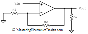
Figure 1 shows the non-inverting amplifier, which drives a load, RL. This circuit has an equivalent Thevenin source as in Figure 2.

non_inverting_amplifier

Figure 1

Read more

Design a Differential Amplifier the Easy Way with Mathcad

For those of you who have Mathcad, designing a differential amplifier is really easy.

Let’s say you need to design a unipolar to bipolar converter and you decide to use a differential amplifier for this task. You know the input and output voltage range and you need to calculate the resistors based on a voltage reference you have in the system. All you have to do is to create a Mathcad file for a quick response. Then store it some place for future designs.

If you would like to know why the unipolar to bipolar converter can be designed with a differential amplifier, read this article, Design a Unipolar to Bipolar Converter for a Unipolar Voltage Output DAC .

Let’s take an example.

Read more

Design a Unipolar to Bipolar Converter for a Unipolar Voltage Output DAC

Unipolar to bipolar converters are useful when we have to have a unipolar component to do a certain job in a mixed signal design environment.  For example, Digital to Analog Converters (DACs) may have the output voltage range 0 to 2.5 V, or 0 to 5 V, while the design asks for a range of –5 V to +5 V.  To comply with this requirement, we have to design a unipolar to bipolar converter which will be inserted between the DAC output and the following bipolar stage.  It looks like the circuit in Figure 1.  How did I design it?

unipolar_to_bipolar_converter_1Figure 1

Read more

Design a Bipolar to Unipolar Converter to Drive an ADC

Most Analog to Digital Converters have a unipolar input that can be a problem when designing bipolar circuits.  Some common ADC input voltage ranges are 0 to 2.5 V, or 0 to 5 V.  However, the analog circuit that drives the ADC can have voltage swings of, –1 V to +1 V, –2 V to +2 V , –5 V to +5 V, and so on.  Bringing the ADC input below ground is a big No-No, because the current from input will flow through the chip substrate creating irreversible changes in the ADC and damage it.  So, how do we connect a bipolar front end circuit with a unipolar ADC?  Enters the bipolar to unipolar converter.  Let’s design one.

The converter can be designed with a summing amplifier, as in Figure 1.  How do we calculate the resistors?

summing_amplifier1

Figure 1

Read more

Show Buttons
Hide Buttons
'