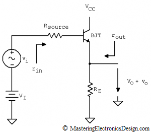
In this article I will show a method to deduce the input and output resistance of the common collector amplifier. The common-collector amplifier is a well known circuit (see Figure 1). It is mostly used as a buffer due to its high input resistance, small output resistance and unity gain. The equations derived in this article are symbolic, as is the derivation of any other formula in this website. Still, even if the resistances’ values are not numeric, the equations are intuitive enough to show the high input, low output resistance property of the amplifier.
Figure 1
The Common-Collector Output Resistance
The output resistance of this amplifier is the resistance seen by the next stage, as looking to the emitter resistor RE, as in Figure 1.
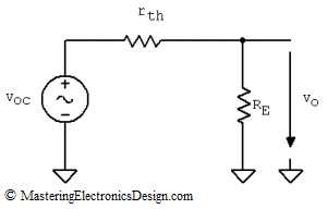
In a previous article, Derive the Transfer Function of the Common Collector Amplifier with Thevenin’s Theorem, I used Thevenin’s Theorem to demonstrate, step by step, how to derive the small-signal transfer function of this amplifier. In the same article, I showed that the common collector amplifier is equivalent to a Thevenin source that feeds RE (see Figure 2).
Figure 2
This source has the open-circuit voltage
and the resistance
The calculation of the common-collector output resistance reduces to the calculation of the output resistance of this circuit, because the two circuits are equivalent.
In Figure 2, voc is an independent source. If we short-circuit this source, the circuit output resistance as seen from RE is RE in parallel with rth. Therefore, rout can be written as in the following equation.
Judging by the usual resistor values of Rsource, r∏ and RE, the ratio (Rsource+r∏)/RE is small as compared to β+1. This shows that RE influence is small in the calculation of the common collector output resistance or, at most, it decreases rth, which is exactly what we need for a circuit output. If we neglect (Rsource+r∏)/RE, rout becomes
which is the equation shown in most articles or textbooks. The output resistance depends mainly on the source resistance Rsource, the transistor input resistance r∏, and it is small, since these two resistor values are divided by a large number, β+1.
The Common-Collector Input Resistance
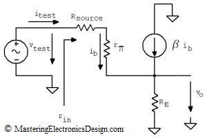
The input resistance is usually calculated with a test source connected at the amplifier input. Its value can be easily derived if we know the test source and the current it sources into the circuit under test. For this task, let’s replace the transistor with its small-signal equivalent as in Figure 3.
Figure 3
According to Ohm’s Law, rinput is calculated by dividing the test source voltage at its current. .
Inspecting the circuit in Figure 3, we can see that itest = ib.
Also, we notice that RE receives two currents, itest and β itest. As such, from vtest, Rsource, r∏, RE loop, vtest can be written as in the following equation:
So the small signal input resistance of the common-collector amplifier is
This equation shows that the common-collector amplifier has a large input resistance, due to the product (β+1) RE. In many texts, Rsource+r∏ is neglected, because it is a lot smaller than (β+1) RE. How small? Rsource can be around 10 kΩ, while r∏, is around 1 kΩ. If RE is 1 kΩ, and β+1 is 200 Ω, one can easily calculate that Rsource+r∏ can be neglected in the rinput equation.
With a small output resistance and a large input resistance, the common-collector amplifier is mostly used as a buffer. As with saw in a previous article, it has a unity gain, making it an ideal circuit to isolate different stages when designing electronic circuits.


this allowed me have an understanding of how to derive the input and output resistance
I understand why you include source resistance in the output resistance equation, but why do you have it in the equation for input resistance? The source resistance is independent of the transistor. The transistor’s input resistance is the load on the source resistance.
Ron, thank you for your comment. I introduced the source load in calculations for 2 reasons.
1. Consistency. Whenever we study the input and output resistance of a network, it is advised by many to always take into consideration the source resistance. This resistance may, or may not, influence the result. In this case, the source resistance does not have any influence on the input resistance. Instead of cherry-picking when to introduce the source resistance and when not, and confuse the readers in the process, better have it in any system study. Readers can easily see that it adds to r-pi and can ignore it if they choose so.
2. Signal accuracy. As figure 3 shows, the calculation of the input resistance is correct, as it is done from the ideal source point of view, through its own resistance. When we look at a stage output signal level, it is actually the level before its own output resistance. This level can be affected by the attenuation created by the source resistance and the input resistance of the following stage. In the case of the common-collector amplifier, the source resistance helps, as it adds to the transistor input resistance.
So, yes, you are right. The source resistance is not part of the transistor input resistance per see. In my opinion it should be there for the reasons I stated.
hi
great tutoriol
i’m matching a simple banpass to a colpits .is transistor output resistance the same as output impedance?
Yes, although, for high frequency applications, I would add the transistor parasitic capacitances in this hybrid-pi model. At minimum, add C-pi in parallel with r-pi and the feedback capacitance C-miu.
thank you for your reply, and apologies for the earlier typos,
as you say, stray capacitances are proving to be a major consideration, ive noticed even on fairly low frequencies, a few hundred kilohertz or so, and with even a 555 on a good layout, im getting a residual capacitance of around 15 p to 20 p on the timing elements.
thanks again
dougal
How about the same type of analysis for the common-base amplifier please?
Yes, it will come soon. Keep an eye on MasteringElectronicsDesign.com. Thank you for visiting.
i thought this have been very helpful. thanks! 😀
why cc has high input resistance
In this article I deduct the input resistance of the common-collector circuit. It is the last equation. The paragraph before the last explains why: “This equation shows that the common-collector amplifier has a large input resistance, due to the product (?+1) RE.” And then it says that if RE is 1k and ?+1 is at least 200, you end up with a large input resistance of at least 200k.
Easy to understand article. Thanks again!!!
I to understand microelectronics. I also think that including the source resistance in the output impedance of the amplifier could be misleading.
1) Isn’t the purpose of the input and output resistances to interface the amplifier with the other blocks so as to to predict the real gain.
If one include the source in the output impedance and the load in the input impedance there is no point in calculating them.
But more importantly, as one goal of the common collector is to adapt a high input impedance from a previous stage (ex: common emitter) to a low output impedance, there is no reason to assume that Rs (=the output impedance of the previous stage) will be small even if it appears divided by beta in the calculation of Ro.
For exemple, imagine a
“I to understand microelectronics. I also think that including the source resistance in the output impedance of the amplifier could be misleading.”
No, it is not. When learning about these simple amplifiers one needs to know that the output impedance depends on the source.