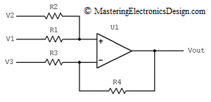
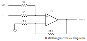
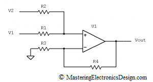
In a comment, one of my readers asked me what is the transfer function of the non-inverting summing amplifier in Figure 1, when R3 is connected to a reference voltage instead of ground. Well, this is a summing amplifier with a differential configuration.
Superposition Theorem
How to Derive the Instrumentation Amplifier Transfer Function
The Instrumentation Amplifier (IA) resembles the differential amplifier, with the main difference that the inputs are buffered by two Op Amps. Besides that, it is designed for low DC offset, low offset drift with temperature, low input bias currents and high common-mode rejection ratio. These qualities make the IA very useful in analog circuit design, in precision applications and in sensor signal processing.
Figure 1
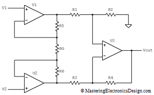
Figure 1 shows one of the most common configurations of the instrumentation amplifier. Its clever design allows U1 and U2 operational amplifiers to share the current through the feedback resistors R5, R6 and RG. Because of that, one single resistor change, RG, changes the instrumentation amplifier gain, as we will see further. RG is called the “gain resistor”. If the amplifier is integrated on a single monolithic chip, RG is usually left outside so that the user can change the gain as he wishes. One example of such instrumentation amplifier is Texas Instruments’ INA128/INA129.
How to Derive the Transfer Function of the Inverting Summing Amplifier
The inverting summing amplifier does exactly what its name says: adds the input signals and inverts the result. This amplifier presents a major advantage versus the non-inverting summing amplifier. The input signals are added with their own gain. The disadvantage is the inversion of the sum, which might not be desirable in some cases.
Figure 1
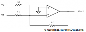
Figure 1 shows the non-inverting summing amplifier with two inputs. Its transfer function is shown in equation (1).
| (1) |
As you can see, this is a simple function. Each signal is added with its own gain created by the feedback resistor, Rf, and the corresponding resistor for that signal. But, why is that? Why is this transfer function a lot simpler than the non-inverting summing amplifier? How can we derive this function? What is the transfer function of the inverting summing amplifier with 3, 4, or n inputs? This article answers all these questions.
The Transfer Function of the Non-Inverting Summing Amplifier with “N” Input Signals
In a previous article, How to Derive the Summing Amplifier Transfer Function, I deduced the formula for the non-inverting summing amplifier with two signals in its input. But what if we have 3, 4 or an n number of signals? Can we add them all with one amplifier?
Theoretically, yes. Practically, it is a different story. There is a practical limit on how many signals can be summed up with one amplifier. When the number of input signals grows, each signal component in the sum decreases in value. By the end of this article you will understand why.
Figure 1
We already saw that, for a summing amplifier with two input signals (Figure 1), the transfer function is
| (1) |
If we need to add 3 signals, the circuit schematic looks like the one in Figure 2. What is the transfer function of this summing amplifier with 3 inputs?
How to Derive the Summing Amplifier Transfer Function
The summing amplifier, or the non-inverting summing amplifier, is an analog processing circuit with the transfer function (the summing amplifier formula as some say) shown in the following equation.
| (1) |
The first term of the product is the actual summing, while the second term is a gain due to the R3 and R4 resistors. I prefer this type of summing amplifier as shown in Figure 1, because it is more flexible and allows us to achieve any linear function we want.
Figure 1
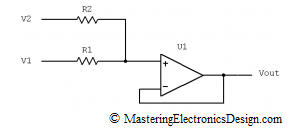
Some authors prefer the following schematic,
Figure 2
with the transfer function
| (2) |
One can see that the summing amplifier in Figure 2 is a subset of my preferred schematic in Figure 1. In Figure 2, R4 is zero, while R3 is infinity (open connection). It performs the analog summation between V1 and V2, with a gain of 1. Therefore, the amplifier in Figure 1 gives us more choices when designing a function with this circuit. If the gain is not needed, this should come up from calculations, as in this article Solving the Summing Amplifier.
If you followed this website, by now you probably figured that I am not a promoter of learning formulas by heart. I like to derive the transfer function if I need it. So, how do we prove this formula?
We will use the Superposition Theorem, which says that, the effect of all the sources in a circuit is equal with the sum of the effects of each source taken separately in the same circuit. Therefore, if we take out one source, V2, and replace it with a wire, we then can find the voltage in each node and the current in each branch of this circuit due to the remaining source V1. Then we do the same with V1 and then sum up the currents on each branch and the voltage levels on each node. We are only interested in Vout, so this should be simple.
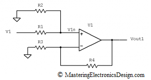
We will first make V2 = 0V, by connecting R2 to ground, as in Figure 3.
Figure 3
The Op Amp is considered an ideal component, so that the input bias currents are negligible. If the current in the non-inverting input is zero, R1 and R2 make a voltage divider for V1. The non-inverting input voltage V1n, can be written as
| (3) |
and, based on the non-inverting amplifier transfer function, Vout1 is
| (4) |
By replacing V1n in (4), the output voltage is
| (5) |
In the second part of my demonstration, based on the Superposition Theorem, R2 is connected back to V2 and V1 = 0, by connecting R1 to ground. Following the same train of thought Vout2 can be written as
| (6) |
Now we have to add Vout1 to Vout2 to complete the third step of the Superposition Theorem. After factorizing the gain component 1+R4/R3, the summing amplifier transfer function becomes the mathematical relation shown in (7).
| (7) |
Q.E.D.
>>> <<<
This formula shows that this sum is a weighted sum between V1 and V2. This is better than a direct sum V1 plus V2, because, again, brings flexibility in design. Together with the differential amplifier, this circuit brings another treat in the art of electronics design.
Converting a Differential Amplifier into a Summing Amplifier
Is there any link between a differential amplifier and a summing amplifier? Yes, it is. They can be easily converted one into the other one. While this article shows the conversion, the main purpose is to demonstrate how the same circuit can be viewed as a differential amplifier or as a summing amplifier, depending on the voltage levels in its inputs.
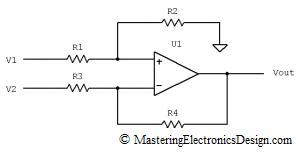
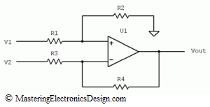
The differential amplifier is shown in Figure 1. It is mostly used to measure the voltage difference between its inputs. In addition, it can be used to achieve a linear function Vout(Vin) (Vout of Vin) where Vout is the voltage at the amplifier output, and Vin is the input voltage. In this case, any one of the inputs V1 or V2 can play the role of Vin. For details, read my articles Solving the Differential Amplifier Part 1, Part 2, and Part 3.
Figure 1
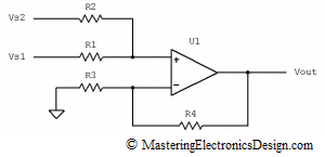
What is interesting about the differential amplifier, which I call a universal amplifier, is that it can be easily converted into a summing amplifier. In fact, they are one and the same circuit. In Figure 2 I drew the summing amplifier, where I noted the voltage levels at its inputs with Vs1 and Vs2. If you would like to read more about the summing amplifier go to this link: Solving the Summing Amplifier.
Figure 2
The differential amplifier can be seen as a summing amplifier, if we look at it differently. If, in Figure 1, we take R2 and move it on the left side of the OpAmp, as in Figure 2, without affecting its connections, the differential amplifier looks like a summing amplifier. The only difference is that, the differential amplifier sums V1 with a zero voltage, because R2 is connected to ground. Also, R3 is connected to V2 instead of being connected to ground.
Therefore, to convert the differential amplifier into a summing amplifier, all we have to do is to adjust the voltage levels as follows:
- Disconnect R2 from ground and connect it to Vs2,
- Connect R3 to ground.
Of course, these steps may be done backwards, if we need to convert a summing amplifier into a differential amplifier.
What about the transfer function of the summing amplifier? Can we easily derive it as well from a differential amplifier transfer function? Of course we can, and here is how.
The differential amplifier transfer function is shown in (1).
| (1) |
As I already said, the differential amplifier is a summing amplifier between V1 and zero volts, and with V2 = 0. Let’s rewrite the transfer function (1) as follows:
| (2) |
Why did I add 0V at V1 times the resistor ratios? Because, as I explained in The Differential Amplifier Transfer Function, any voltage on the non-inverting input multiplies the R4, R3 ratio plus one.
Now, if we connect R1 to Vs1 and connect R2 to Vs2, the transfer function becomes
| (3) |
where by k I noted the resistor ratio for Vs2. Using the Superposition Theorem, we realize that Vs2 “sees” a voltage divider made by R1 and R2, with the ratio of
| (4) |
For details on how to determine this ratio, read my article How to Derive the Summing Amplifier Transfer Function.
Replacing k in equation (3), we arrive at the summing amplifier transfer function as shown in equation (5).
| (5) |
Q. E. D.
The Differential Amplifier Common-Mode Error – Part 1
The common-mode voltage can bring errors in the differential amplifier applications. What is the common-mode voltage? The common-mode voltage is the voltage level common to both inverting and non-inverting inputs of the differential amplifier. In many applications, the differential amplifier is used to amplify the difference between two voltages, for later processing, or to isolate a signal from common-mode noise, or to amplify a signal that rides on top of some large voltage level. If the common-mode voltage is not rejected, it appears as an error at the amplifier output.
It is customary to consider the common-mode error as being negligible, based on the high Common-Mode Rejection Ratio (CMRR) of the operational amplifiers. This is not always the case. Once the electronics designer connects resistors around this amplifier, in a differential configuration, the common-mode error starts to be significant.
The common-mode voltage Vcm and the differential voltage Vd are shown in the group of equations (1).
| (1) |
Why these expressions? How was Vcm defined like that and why? We will start by looking at the significance of each input voltage in the differential amplifier.
Looking at Figure 1, V1 is the input voltage between R1 and ground, while V2 is the input voltage between R3 and ground.
Figure 1
As we saw in MasteringElectronicsDesign.com: The Differential Amplifier Transfer Function, the signal at the amplifier output is as follows:
| (2) |
If we arrange this equation differently, as in (3),
 |
(3) |
one can see that, in the unique case in which
| (4) |
the circuit amplifies the difference of the input signals, V1-V2. In other words,
| (5) |
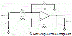
So, which is the common-mode voltage? In order to give you an answer, let’s rearrange the input signals as in Figure 2.
Figure 2
It should be clear now that, when the ratio of the resistor pairs is equal, V2 contribution to the output signal is zero. This can also be seen from equation (2) written differently, as in (6). In equation (6), I grouped the terms so that two main signals are shown: the difference V1-V2 and V2.
 |
(6) |
How did I arrive at this equation? It can be done in two ways: mathematically, using simple algebra methods, or, by using the Superposition Theorem.
Using the Superposition Theorem is easier, because we can consider that there are two voltage sources in the circuit in Figure 2. One source is V1-V2 and the other one is V2. Based on the Superposition Theorem if we take out one source, V2, and replace it with a wire, we find the first term of equation (6). Indeed, when R3 is connected to ground, the amplifier in Figure 2 becomes a non-inverting amplifier. As I showed in a previous article, MasteringElectronicsDesign.com: The Differential Amplifier Transfer Function, Vout1 is the voltage at the non-inverting input times the gain given by R4 and R3.
| (7) |
With Vout1 I noted the output voltage when V2 is zero.
By rearranging
 we arrive at the first term of equation (6).
The second term of equation (6) is the output voltage when V1-V2 is made zero. In this case the amplifier in Figure 2 is a differential amplifier with the same voltage, V2, at both inputs. Hence, the second term of equation (6).
Equation (6) is important because it shows the common-mode error. Since the circuit amplifies the difference V1-V2, this signal appears as riding on top of V2. Hence, V2 can be seen as a common-mode voltage. If the resistor ratios are rigorously equal, the second term in equation (6) is zero. If they are not, the same term will show up at the amplifier output as an error. This is the common-mode voltage error.
How big is this error and why should the electronics designer be concerned about it?
Let’s consider that the ratio of the resistors is equal, as in equation (4), and that only R2 has a tolerance t which can be positive or negative, but smaller than 20%. In other words:
| (8) |
For resistors, this is a practical assumption. Examples of usual resistor tolerances are 0.1%, 1%, 10%, 20%. In my example R1, R3 and R4 are ideal resistors, with 0 tolerance, while R2 has a tolerance of, say, 10% which I noted with t. This creates a mismatch in the resistor ratios R2/R1 and R4/R3 , so that the common-mode voltage V2 appears at the differential amplifier output, scaled by a factor dependent on the tolerance t. This voltage level is the common-mode error.
To calculate this error, let’s write the common-mode portion of the differential amplifier output by taking into consideration the tolerance t of resistor R2,
 |
(9) |
where with Vocm I noted the common-mode voltage at the differential amplifier output. Since the signal of interest is the difference V1-V2, the common-mode error at the differential amplifier output is Vocm.
After calculations, and using (4), Vocm becomes
 |
(10) |
We can consider that t·R2/R1 is small compared with the ratio R2/R1 which determines the gain of the amplifier. Also, for gains larger than 10, the value of 1 in the denominator can be neglected. Therefore, the common-mode error Vocm is
| (11) |
Equation (10) shows that, if one resistor, R2, has a tolerance other than zero, there is a significant error at the differential amplifier output, which is approximately the common-mode voltage times that tolerance.
As an example, if V2 = 10V, V1 = 10.1V, and
the circuit in Figure 1 amplifies the difference between these two signals, so that the output is 2V.
However, if R2 has a tolerance of +10%, the error at the circuit output is Vocm = 10V·0.1 = 1V. As a result, the differential amplifier output will be the sum of the differential output of 2V and the error of 1V, which makes 3V. The error of 1V is significant.
If R2 has a tolerance of 0.1%, the error is 10mV, which can be considered negligible in some applications. That is why the usual recommendation is to have either highly matched resistors for the differential amplifier, or resistors with 0.1% or even 0.05% tolerance.
The same logic is valid for V1 that can be viewed as the common-mode voltage, while the circuit amplifies the negative difference -(V1-V2). In the next part I will show that the convention for the common-mode voltage is
and also the reason why this is the preferred method.


