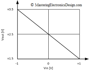
Sometimes all we know about a circuit is its transfer function graph. The transfer function might look like the one in Figure 1. How can we design a circuit so that its input-output behavior will match the graph?
The design starts with the mathematical form of the transfer function. This is a linear function, with the general form of a first order polynomial function.
| (1) |
where (x1,y1) and (x2,y2) are two arbitrary points on the linear graph.
So, let’s write this function for the graph in Figure 1. The pair (x1,y1) can be (-1V,+3.5V) and (x2,y2) can be (+1V, +1.5V), which are input/output voltage levels for our circuit. Replacing x1, y1, x2, y2 in equation (1), and replacing y with Vout and x with Vin, the transfer function is as follows:
| (2) |
or
| (3) |
where Vout is the circuit output signal in volts and Vin is the input signal.
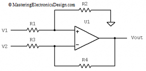
Now comes a little bit of reasoning. The transfer function (3) represents the given graph in Figure 1. How can we create a circuit to resemble this function? Well, if you browse through this article Useful Operational Amplifier Formulas and Configurations, you can see that the differential amplifier has exactly this format. The first term is positive and the second is negative as in the following equation:
| (4) |
The proof of this transfer function can be found here: How to Derive the Differential Amplifier Transfer Function.
Math tell us that two linear functions are identical when their coefficients are identical. Therefore, let’s write the coefficients identities in the form of a system of equations:
 |
(5) |
In this system I considered that Vin is V2 in equation (4), in other words, we are going to connect the input signal to R3 (see Figure 2).
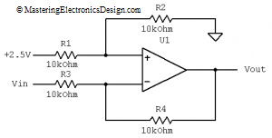
This system is easy to be solved. It is a system of 2 equations with 2 unknowns: R4/R3 and R1/R2. From the system second equation the ratio R4/R3 is already given as equal with one. We can choose R3 = R4 = 10 kOhms.
For V1 we can choose some reference voltage we have available in the project. Let’s say V1 = 2.5V. By replacing R4/R3 in the system first equation, and after calculations, R1/R2 = 1 and R1 = R2 = 10 kOhms.
Here is the circuit we just designed starting with its transfer function:


how would i graph the analog function represented by a sequence of binary numbers…
You have to give me more details to help you. A bi-dimensional graph has 2 axes. The sequence of binary numbers is on one axis. What is on the other? For example. if the sequence of binary numbers comes from an ADC, on one axis there are these numbers, and on the other axis the ADC input voltage. You can see such a graph in this article, An ADC and DAC Integral Non-Linearity (INL), figure 1.
This is a good method but I am looking for something in terms of the laplace operator… I specifically need a circuit that will do the exact behavior in the following transfer function (link)…I am not sure where to start:
http://lpsa.swarthmore.edu/Bode/Example3/index.html
Is there any way to start from here?
That transfer function shows that the amplifier has reactive elements, like capacitors, besides resistors. What I showed in this article is the DC calculation of a circuit, starting from its linear transfer function. Discussing the function you pointed to, takes more than just this comment space. Since you mentioned it, I will most likely write an article about it. Check back from time to time or subscribe to this website.
Thanks a lot for your great website, very clear and detailed.
I might be wrong (I hope not..) but from your graph I see the transfer function:
Vout = Vin + 2.5
Since you followed your demonstration using the equation Vout = -Vin + 2.5 it might just be the graph, where I would expect to see a line from top left corner to bottom right corner.
Best,
Adrien
Thank you for your comment. You are right, the graph should have a negative slope. I made the correction.