Useful Operational Amplifier Formulas and Configurations

My friends advised me that it would be helpful to have on this site the most common operational amplifier configurations and transfer functions or formulas.  So, here they are.  This article is not just a simple collection of circuits and formulas.  It also has links to the transfer function proof for these circuits so I hope it will be very helpful.  Make sure you post a comment and let me know how I can improve this page.  This article will be updated, so do check it often.

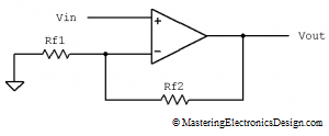
Non-inverting Amplifier

non-inverting-amplifier-1

image0022

Note:  The proof of this transfer function can be found here:  How to Derive the Non-Inverting Amplifier Transfer Function.

Voltage Follower

voltage-follower-2

image0041

Note:  This configuration can be considered a subset of the Non-inverting Amplifier.  When Rf2 is zero and Rf1 is infinity, the Non-inverting Amplifier becomes a voltage follower.  When a resistor has an infinity value, in practice it means it is disconnected.

Read more

How to Derive the Transfer Function of the Inverting Summing Amplifier

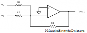
The inverting summing amplifier does exactly what its name says: adds the input signals and inverts the result.  This amplifier presents a major advantage versus the non-inverting summing amplifier.  The input signals are added with their own gain.  The disadvantage is the inversion of the sum, which might not be desirable in some cases.

inverting_summing_amplifier_1

Figure 1

Figure 1 shows the non-inverting summing amplifier with two inputs.  Its transfer function is shown in equation (1).

image0021 (1)

As you can see, this is a simple function. Each signal is added with its own gain created by the feedback resistor, Rf, and the corresponding resistor for that signal.  But, why is that?  Why is this transfer function a lot simpler than the non-inverting summing amplifier?  How can we derive this function?  What is the transfer function of the inverting summing amplifier with 3, 4, or n inputs?  This article answers all these questions.

Read more

The Transfer Function of the Non-Inverting Summing Amplifier with “N” Input Signals

In a previous article, How to Derive the Summing Amplifier Transfer Function, I deduced the formula for the non-inverting summing amplifier with two signals in its input.  But what if we have 3, 4 or an n number of signals?  Can we add them all with one amplifier?

Theoretically, yes.  Practically, it is a different story.  There is a practical limit on how many signals can be summed up with one amplifier.  When the number of input signals grows, each signal component in the sum decreases in value. By the end of this article you will understand why.

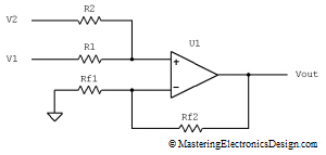
summing_amplifier_1

Figure 1

We already saw that, for a summing amplifier with two input signals (Figure 1), the transfer function is

image002 (1)

If we need to add 3 signals, the circuit schematic looks like the one in Figure 2.  What is the transfer function of this summing amplifier with 3 inputs?

Read more

An ADC and DAC Differential Non-Linearity (DNL)

As in the case of INL, DNL is an important parameter of an ADC or DAC because it is a measure of their non-linearity.  DNL stands for Differential Non-Linearity and quantifies the ADC or DAC precision.

The term differential refers to the values an ADC takes between two consecutive levels.  When the input signal swings in any direction, the ADC samples the signal and its output is a stream of binary numbers.  An ideal ADC will step up or down one Least Significant Bit (LSB), without skipping any level and without holding the same decimal number past two or three LSBs. However, due to technological limitations, ADCs and even DACs are not ideal.  When that happens, the ADC’s linearity is severely impacted.  Therefore, DNL is defined as the maximum deviation from one LSB between two consecutive levels, over the entire transfer function.

In an electronic system, linearity is important.  When an ADC is non-linear, it brings imprecision in measurements.  If a DAC is non-linear, it restores a dynamic signal with high distortions.  Moreover, an accumulation of skipped levels, or high DNL, can increase the INL as well.

Figuring out the DNL value is quite simple. One has to measure the ADC response to a voltage value that would correspond to one LSB. For example, if we have a 12-bit ADC and the voltage reference is 2.5V, one LSB is given by the following equation.

image001

So, for each 0.6103 mV increase in the ADC input, the output hexadecimal value will increase with one.

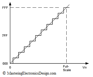
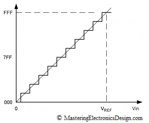
figure-1

Figure 1

An ideal ADC transfer function is shown in Figure 1.  This is a 12-bit ADC, but the steps are exaggerated for better viewing.  There is no deviation from 1 LSB step, so the DNL is zero.

figure-2_2

Figure 2

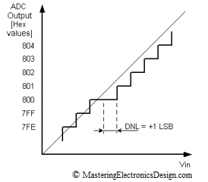
In Figure 2, the ADC holds the 0x800 hex output for two full steps. Since the deviation is towards the positive values on the X scale, and the ADC output holds the same value for an extra LSB, the Differential Non-Linearity is +1 LSB.

figure-2_3

Figure 3

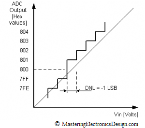
Figure 3 shows that the DNL migrated towards negative values for one LSB. Therefore, DNL in Figure 3 is -1 LSB. Since 0x800 is missing, there the ADC is categorized with missing codes.  Such an ADC cannot be used for high precision applications.

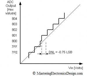
The DNL in Figure 4 is -0.75, because the 0x800 is still there, but for a shorter voltage range than one LSB.  The code is still there, so the ADC can be used in precision applications.

figure-3_2

Figure 4

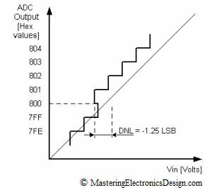
In Figure 5, the 0x800 step appears at lower voltage inputs than one LSB.  The DNL is -1.25 LSB. It is clear that the ADC is highly non-linear.  Moreover, it is categorized non-monotonic.  High DNL values, positive or negative can increase the INL as well.

figure-2_4

Figure 5

A non-monotonic DAC is highly undesirable, especially if the DAC is used in a closed loop application like servo or process controls.  With a non-monotonic DAC the system may become unstable, or the control may suffer from jumpiness, jitteriness and overall difficult control handling.

The main rule for precision applications is to choose a component with a DNL less than one LSB. In this case, the ADC or DAC is assured monotonicity, no missing codes and a good linearity.

An ADC and DAC Integral Non-Linearity (INL)

What is INL?  This term describes the non-linearity of Analog to Digital Converters (ADC) and Digital to Analog Converters (DAC).  INL stands for Integral Non-Linearity.  Is this term important? Should we be concerned about this specification?  The answer is yes.

INL is considered an important parameter because it is a measure of an ADC or DAC non-linearity error.  However, as in any Analog or Mixed-Signal Design project, some specifications are important, some are not.  It all depends on the project requirements regarding accuracy and precision.  Understanding INL enables the circuit designer to avoid surprises in his or her project.

The Integral Non-Linearity is defined as the maximum deviation of the ADC transfer function from the best-fit line.  An ADC function is to digitize a signal into a stream of digital words called samples.  The ADC output is discrete as opposed to the input, which is continuous.  It is used at the boundary between the analog and digital realms.

The ADC input is usually connected to an operational amplifier, maybe a summing or a differential amplifier which are linear circuits and process an analog signal.  As the ADC is included in the signal chain, we would like the same linearity to be maintained at the ADC level as well.  However, inherent technological limitations make the ADC non-linear to some extent and this is where the INL comes into play.

figure-1

Figure 1

Figure 1 shows the ADC transfer function.  For each voltage in the ADC input there is a corresponding word at the ADC output.  The figure shows a 12-bit ADC where the steps were exaggerated for better viewing.  The y axis, the output, is digital, so that the values are represented in hexadecimal format.  If the ADC is ideal, the steps shown are perfectly superimposed on a line.

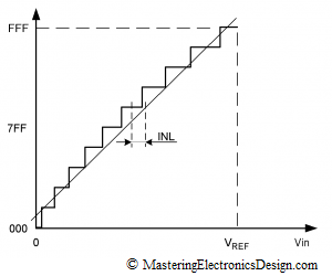
figure-2

Figure 2

Figure 2 shows an ADC with a slight non-linearity.  To express the non-linearity in a standard way, manufacturers draw a line through the ADC transfer function, called the best fit line.  The maximum deviation from this line is called INL, which can be expressed in percentage of the full scale or in LSBs (List Significant Bit). INL is measured from the center of each step to that point on the line, where the center of the step would be if the ADC was ideal.

This parameter is important because it cannot be calibrated out.  The ADC non-linearity is unpredictable.  We don’t know where on the ADC scale the maximum deviation from the ideal line is.  Therefore, if one of the design requirements is good accuracy, we need to choose an ADC with the INL within the accuracy specifications, or a lot less than the specified error.

For example, let’s say the electronic device we design has an ADC that needs to measure the input signal with a precision of 0.5% of full-scale.  Due to the ADC quantization, if we choose a 12-bit ADC, the initial measurement error is +/- 1/2 LSB which is called the quantization error.

image0031

With the ADC quantization error almost 40 times lower than the design requirements, a 12-bit ADC can do a good job for us.  However, if the INL is large, the actual ADC error may come close to the design requirements of 0.5%.  We would like to keep each component error in the circuit as low as possible, so that the total combined error of the electronic device we design is less than 0.5%.  Gain or offset errors in an ADC can be calibrated out, but INL cannot.  If we need to live with an evil, at least we need to choose an ADC with a small INL.  This may increase the cost we allocate for the ADC in the system, but it is worthwhile if we are to keep our promises and design a device within specifications.

The DAC Integral Non-Linearity can be viewed the same as for an ADC.  The only difference is that, with a DAC, the INL may not be as important.  If the DAC is used to set a few voltage levels in a system, those values may be easily calibrated, so we can choose a low cost DAC.  However, if the DAC is used to accurately restore a dynamic signal, the INL cannot be easily calibrated.  In that case, we need to choose a high precision DAC, with a good INL.

It’s an Analog World by Design

My daughter, Laura, a lawyer now, asked me, what is Analog?  What is Mixed-Signal Design?  She is very familiar with the word digital.  Like many people I know who are professionals in other areas than Electronics, she was born in a digital world or got very accustomed to this word.  This is mostly due to the fact that digital, as a concept, is/was overused in the consumer market.  Today we buy digital TV sets, while the analog ones were popularized as being old.  In with the new, out with the old, right?  The analog TV bands were, well “disbanded” (pun intended), and are allocated now to digital devices.  We moved from the analog LPs (vinyl discs) to CDs (digital compact discs).  The land telephone was redesigned digital, and the new telephone, the cell phone, was invented directly in digital format.

It seems that everything around us is digital nowadays.  Then, why these words, “It’s an Analog World by Design”?  Why is the world analog and, what is analog?

Well, the world is what it is.  No matter your beliefs regarding how the world was created, the world exists and we, as humans, are passersby in this world.  We have to adapt to this world and take it as is in its complexity and self-reliance.  In order to survive in this world we rely on our sensors.  Whether they are optical, auditive, tactile, visual, we need these sensors to connect to our world.  Our sensors are limited.  For example, we can only hear signals within a very small portion of frequencies from about 12 Hz to 20000 Hz, out of a very large number of frequencies in the Universe.  We call this band of frequencies sound.  We can only see signals with wavelengths from 380 nm to 740 nm and this spectrum spread we call light.  We are limited in our perception, but these sensors are good enough for us.  For the rest of the signals, we build electronic equipment to enhance our sensors.

The signals we receive from Mother Nature are continuous.  We don’t hear any discontinuity or choppiness in the sounds of ocean waves or bird songs and this is what makes the world analog.  From our point of view, with the sensors we have, we interact with our world continuously.  The signals have amplitude that can vary in time and are composed of a complex of frequencies.

So how is Analog defined?  Merriam-Webster dictionary reads that analog is “of, relating to, or being a mechanism in which data is represented by continuously variable physical quantities.”  The word comes from the ancient Latin, analogus, or Greek, analogos, meaning proportional.  The term was adopted most likely because the continuous signal we perceive is proportional to another continuous signal;  or the signal has to be proportionate with itself at every point in time, so that leaves room for no discontinuity;  or, the notion might have had a mathematical approach to the Intermediate Value Theorem that states that, if a real function is defined on a closed interval [a,b], and k is a number in the interval [f(a),f(b)], the function is continuous if there is a number c in the interval [a,b] so that f(c) = k.  The intermediate values can be construed as being proportional to other intermediate values in the function’s domain, when there is no discontinuity.

No matter the reason for which the word analog was associated with continuous electrical signals, the analog domain and the analog design are here to stay because we live in a continuous world as we perceive it.  The interface between our world and our instruments and electrical equipment has to be analog.  We need to capture the sound with a microphone, which is analog.  We need to send electrical signals into a speaker, which is analog.  We need to measure the temperature with a sensor, which is analog.  We need to measure the optical light with a sensor, which is analog.

We need to amplify and filter the signals we capture with these sensors, to be able to digitize and process them in the digital domain.  Amplification, filtering, addition, multiplication in analog domain and the circuits we achieve these operands and tasks with, are called Analog Signal Processing.

Analog signals and analog processing have their own limitations and that is why we digitize the signals, for an error free transmission, correction, easy storage, sharp filtering and many other reasons.  The design of the circuits that handle the signals between the analog and digital domains is called Mixed-Signal Design.

The design of the electronic circuits that manage the analog processing is very subjective.  There are many ways to handle different tasks in the analog domain, but not all are seen as being elegant or high-end solutions.  This is where the real talent comes in place and where the knowledge, expertise and experience of the analog designer have a say.  Because of that, the analog and mixed-signal design became an art.

The design cannot be automated as with the digital circuits.  Sure, there are computer tools like SPICE based programs, which can verify and calculate the analog design, but the schematics have to be created by a human being in the first place.  Maybe that is why we have so many computer tools to automatically create digital circuits, while the analog tools are still to be invented.  Human creativity is difficult to be automated.  Maybe a distant future, when artificial intelligence will approach creativity, might be able to automatically create analog circuits.  But, will it?

How to Derive the Summing Amplifier Transfer Function

The summing amplifier, or the non-inverting summing amplifier, is an analog processing circuit with the transfer function (the summing amplifier formula as some say) shown in the following equation.

image001 (1)

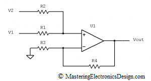
The first term of the product is the actual summing, while the second term is a gain due to the R3 and R4 resistors.  I prefer this type of summing amplifier as shown in Figure 1, because it is more flexible and allows us to achieve any linear function we want.

summing_amplifier1

Figure 1

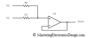
Some authors prefer the following schematic,

summing_amplifier2

Figure 2

with the transfer function

image0041 (2)

One can see that the summing amplifier in Figure 2 is a subset of my preferred schematic in Figure 1.  In Figure 2, R4 is zero, while R3 is infinity (open connection).  It performs the analog summation between V1 and V2, with a gain of 1.  Therefore, the amplifier in Figure 1 gives us more choices when designing a function with this circuit.  If the gain is not needed, this should come up from calculations, as in this article Solving the Summing Amplifier.

If you followed this website, by now you probably figured that I am not a promoter of learning formulas by heart.  I like to derive the transfer function if I need it. So, how do we prove this formula?

We will use the Superposition Theorem, which says that, the effect of all the sources in a circuit is equal with the sum of the effects of each source taken separately in the same circuit.  Therefore, if we take out one source, V2, and replace it with a wire, we then can find the voltage in each node and the current in each branch of this circuit due to the remaining source V1.  Then we do the same with V1 and then sum up the currents on each branch and the voltage levels on each node.  We are only interested in Vout, so this should be simple.

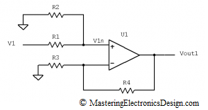
We will first make V2 = 0V, by connecting R2 to ground, as in Figure 3.

summing_amplifier3

Figure 3

The Op Amp is considered an ideal component, so that the input bias currents are negligible.  If the current in the non-inverting input is zero, R1 and R2 make a voltage divider for V1.  The non-inverting input voltage V1n, can be written as

image0061 (3)

and, based on the non-inverting amplifier transfer function, Vout1 is

image0071 (4)

By replacing V1n in (4), the output voltage is

image0082 (5)

In the second part of my demonstration, based on the Superposition Theorem, R2 is connected back to V2 and V1 = 0, by connecting R1 to ground.  Following the same train of thought Vout2 can be written as

image0091 (6)

Now we have to add Vout1 to Vout2 to complete the third step of the Superposition Theorem.  After factorizing the gain component 1+R4/R3, the summing amplifier transfer function becomes the mathematical relation shown in (7).

image001 (7)

Q.E.D.

>>>  <<<

This formula shows that this sum is a weighted sum between V1 and V2.  This is better than a direct sum V1 plus V2, because, again, brings flexibility in design.  Together with the differential amplifier, this circuit brings another treat in the art of electronics design.

Show Buttons
Hide Buttons
'