Open-loop, Closed-loop and Feedback Questions and Answers

One of my readers posted the following questions in the comment section of MasteringElectronicsDesign.com: An Op Amp Gain Bandwidth Product.

I am doing a work on fully differential Negative feedback op-amp with capacitive divider configuration. I have some questions and confusions, can you please clarify?

What is the difference between closed loop gain and open loop gain, and are they dependent to each other?

How can we calculate the unity gain frequency if I have a 3-dB frequency of 100Hz and closed loop gain of 40dB?

Does the feedback factor (BETA) has importance with respect to any other parameters?

How will it help in finding the closed transfer function of the system assuming the op-amp as a single pole system?

The answers needed some space, more than the comment section could offer, so here is a post on the topics of op amp open-loop, closed-loop and feedback.

Read more

An Ideal Operational Amplifier Simulation Model

You worked hard on your schematic, you calculated everything, you feel confident that it will work.  To be sure though, before committing the schematic to copper, you want to simulate it.  You develop a SPICE simulation schematic and, surprise, things don’t work.  What’s going on?

You start searching for bad connections in the simulation schematic.  You check the power supplies and the circuit biasing.  Finally, in desperation, you suspect the operational amplifier model that you downloaded from the manufacturer website, or found in the SPICE program library.  How do you troubleshoot your circuit?

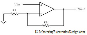
First, split your circuit into small subcircuits, like a one op amp circuit.  Second, take aside, on a different simulation page, one of these subcircuits.  Is that working?  If that circuit is a non-inverting amplifier, as an example (Figure 1), and the output voltage is all over the place except your expected value, than replace your op amp with an ideal one and see if that circuit works.

Read more

Design a Bipolar to Unipolar Converter with a 3-input Summing Amplifier

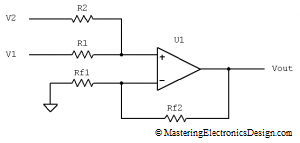
Since the publication of Design a Bipolar to Unipolar Converter to Drive an ADC, several readers contacted me with requests to help in solving their particular converter. The common problem they had was the fact that the components’ calculation resulted in a negative value for at least one resistor.

To provide a solution, first we need to understand the root cause of the problem. Let’s take one of the circuits I received and analyze it.

The reader wrote that he would like to drive an ADC with the input range of 0 to 2.5V from a signal with the range of –5V to +5V, connected at V1 (see Figure 1).

Read more

The Non-Inverting Amplifier Output Resistance

It is customary to consider the output resistance of the non-inverting amplifier as being zero, but why is that? An Op Amp’s own output resistance is in the range of tens of ohms. Still, when we connect the Op Amp in a feedback configuration, the output resistance decreases dramatically. Why?

To answer these questions, let’s calculate the output resistance of the non-inverting amplifier.

It is widely accepted that the output resistance of a device can be calculated using a theoretical test voltage source connected at the device output. The input, or inputs, are connected to ground. Nevertheless, instead of using this method, let’s try a different one: The small signal variation method.

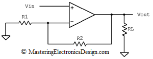
Figure 1 shows the non-inverting amplifier, which drives a load, RL. This circuit has an equivalent Thevenin source as in Figure 2.

non_inverting_amplifier

Figure 1

Read more

Useful Operational Amplifier Formulas and Configurations

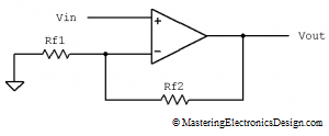
My friends advised me that it would be helpful to have on this site the most common operational amplifier configurations and transfer functions or formulas.  So, here they are.  This article is not just a simple collection of circuits and formulas.  It also has links to the transfer function proof for these circuits so I hope it will be very helpful.  Make sure you post a comment and let me know how I can improve this page.  This article will be updated, so do check it often.

Non-inverting Amplifier

non-inverting-amplifier-1

image0022

Note:  The proof of this transfer function can be found here:  How to Derive the Non-Inverting Amplifier Transfer Function.

Voltage Follower

voltage-follower-2

image0041

Note:  This configuration can be considered a subset of the Non-inverting Amplifier.  When Rf2 is zero and Rf1 is infinity, the Non-inverting Amplifier becomes a voltage follower.  When a resistor has an infinity value, in practice it means it is disconnected.

Read more

The Transfer Function of the Non-Inverting Summing Amplifier with “N” Input Signals

In a previous article, How to Derive the Summing Amplifier Transfer Function, I deduced the formula for the non-inverting summing amplifier with two signals in its input.  But what if we have 3, 4 or an n number of signals?  Can we add them all with one amplifier?

Theoretically, yes.  Practically, it is a different story.  There is a practical limit on how many signals can be summed up with one amplifier.  When the number of input signals grows, each signal component in the sum decreases in value. By the end of this article you will understand why.

summing_amplifier_1

Figure 1

We already saw that, for a summing amplifier with two input signals (Figure 1), the transfer function is

image002 (1)

If we need to add 3 signals, the circuit schematic looks like the one in Figure 2.  What is the transfer function of this summing amplifier with 3 inputs?

Read more

Show Buttons
Hide Buttons
'